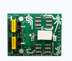
Engineered to support thick copper traces and high thermal stress in specialized Finland industrial grids and renewable applications.
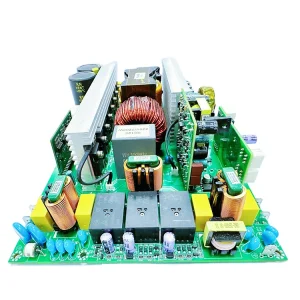
Thick Copper Printed Circuit Boards (PCBs), historically categorized as circuit boards containing more than 3 ounces (oz) of copper per square foot, represent the structural backbone of power electronics. In cold-climate, high-efficiency industrial ecosystems like Finland, the demands placed on these boards are far more stringent than standard commercial electronics. Heavy copper designs (typically scaling from 4 oz up to 20 oz of copper thickness) are imperative for managing intense currents, distributing load, and eliminating hot spots inside sealed enclosures operating in extreme environment zones.
Finland stands at the global forefront of high-technology industrial engineering, clean energy systems, and electrification. From offshore wind farms along the Gulf of Bothnia to the massive marine propulsion engines built in Turku and Vaasa, Finnish OEMs demand electrical solutions that guarantee 100% operational uptime. The climatic conditions of the Nordic region, characterized by deep winters and high humidity cycles, subject electronic equipment to rapid thermal expansion and contraction. Heavy copper PCBs are utilized because they minimize mechanical failures induced by coefficient of thermal expansion (CTE) mismatches under sub-zero temperatures.
Furthermore, Finland’s national grid targets carbon neutrality rapidly, driving immense investments in electric vehicle (EV) fast-charging infrastructure (featuring high current loads up to 350 kW), solar inverters, and high-voltage grid substations. System integrators across Helsinki, Espoo, Tampere, and Oulu are seeking dependable fabrication partners capable of handling advanced heavy copper stackups with Tg (Glass Transition Temperature) values over 170°C and specialized resin-filling processes to prevent delamination.
For global procurement managers, obtaining heavy copper boards from reliable suppliers requires balancing specialized engineering and manufacturing capabilities. Unlike standard FR4 PCBs, thick copper manufacturing processes require deep chemical etching controls and specialized multi-cycle lamination. Under-etching leads to shorts, while over-etching reduces the conductor cross-section, threatening catastrophic thermal runaway in heavy-current designs.
Key global procurement demands include:
Thick copper traces act as integrated heat sinks. By increasing the copper volume, thermal energy is conducted away from critical power components (such as MOSFETs, IGBTs, and diodes) directly into the board and external cooling systems. This drastically reduces the dependency on heavy external heat sinks, lowering the overall weight and footprint of the final unit.
Heavy copper layers permit high current densification within multi-layer formats. This minimizes electrical resistance and trace impedance, reducing resistive power losses (I²R losses) and preventing thermal decay of the surrounding dielectric layers.
Bridging the gap between heavy power distribution and complex signal integration.
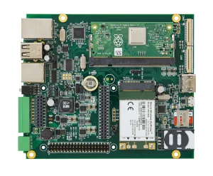
As power conversion systems become more compact, the industry is transitioning from single-layer thick copper architectures to complex Multi-layer Hybrid Copper Boards. In these hybrid boards, the outer layers carry thick copper traces (up to 12 oz) for massive current routing, while the inner layers feature standard copper weights (1 oz to 2 oz) to route high-speed signals or logic commands. This eliminates the need for separate control cards, reducing connector failure points and improving overall signal integrity.
Moreover, the integration of Embedded Busbars represents the next stage of power PCB evolution. Rather than using external copper busbars, copper profiles are embedded directly into pre-routed cavities inside the multilayer board, allowing for seamless transition from logic circuits to heavy-duty power terminals.
Another major trend is the development of ultra-reliable thermal interfaces. Utilizing ceramic-filled dielectric materials alongside thick copper cladding enables superior performance in high-temperature environments. In Finland’s mining machinery and harsh industrial automation sectors, these innovations ensure that electronics can operate continuously without experiencing degradation from mechanical vibration or rapid thermal shock.
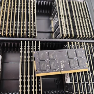
Your Global Manufacturing Partner for Advanced Industrial Electronics and Memory Solutions
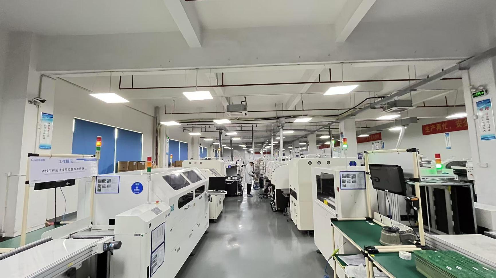
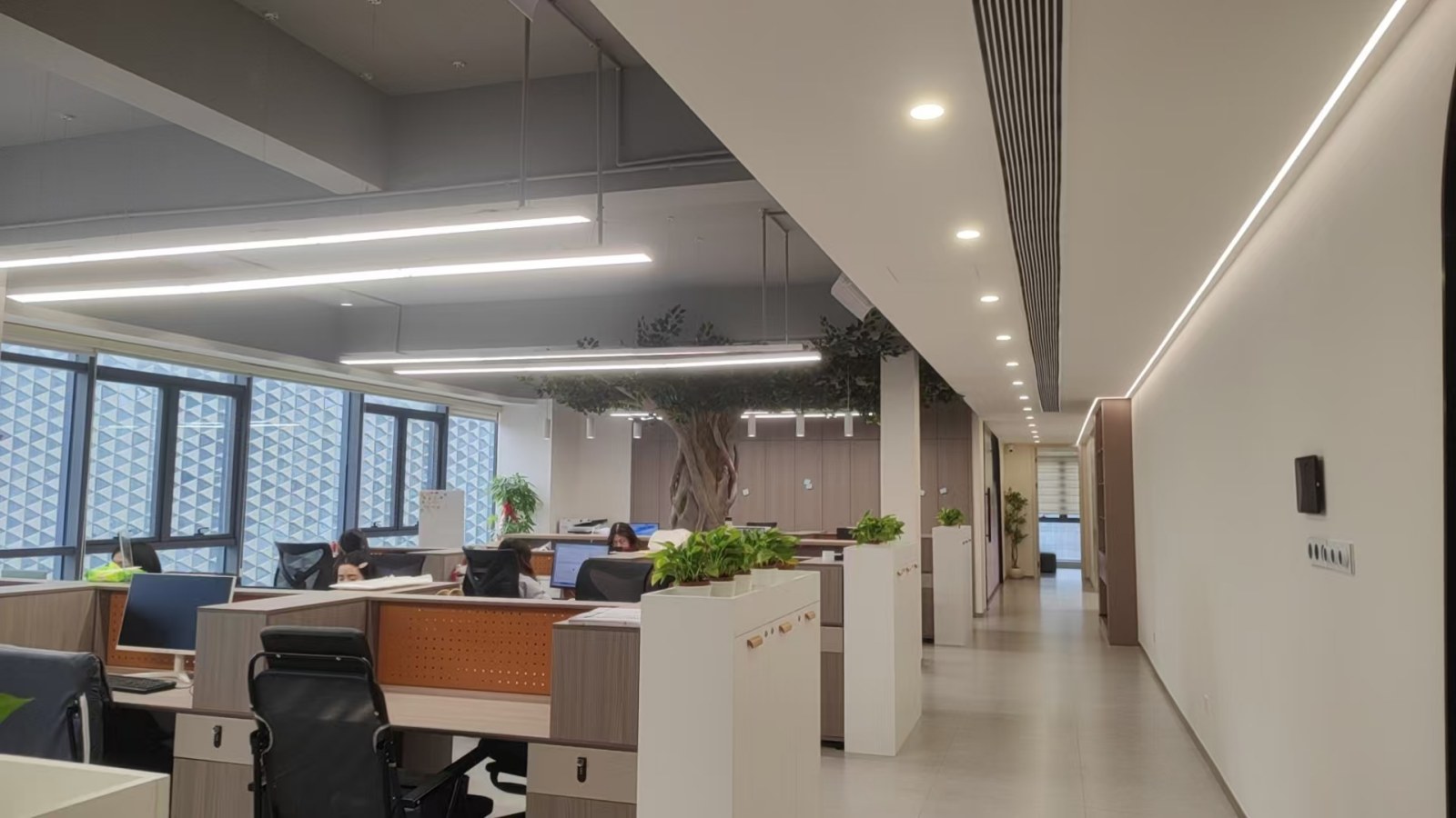
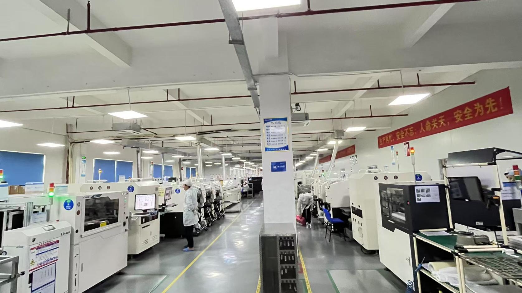
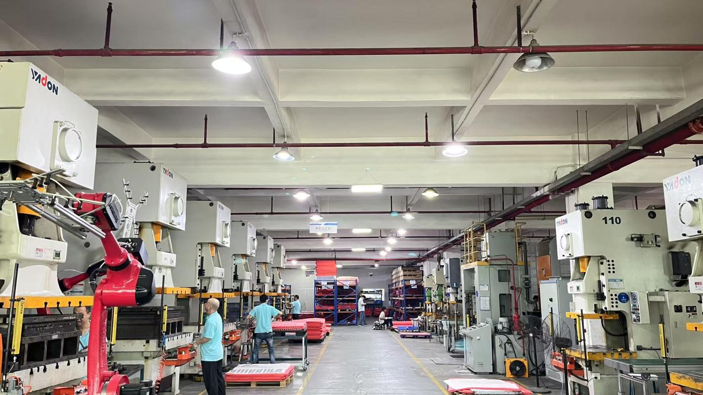
Founded in 2016, Vorynex Memory Technology (China) Co., Ltd. has established itself as an engineering-driven OEM/ODM solutions provider for complex, high-performance computing, memory modules, and high-reliability industrial printed circuit board assemblies. With a modern, highly controlled production facility spanning approximately 320㎡ and utilizing state-of-the-art automated optical inspection (AOI) and in-circuit testing (ICT), we maintain a rigid standard of quality control.
Backed by over 12 years of industry experience in semiconductors and electronics engineering, alongside 6 years of international trade experience, Vorynex achieves an annual export revenue of over USD 12 million. We collaborate with more than 1,200 trusted supply chain partners to source only the highest grade components, ensuring that every batch of PCBs and memory modules complies with global certifications (CE, RoHS, FCC).
Our engineering team, consisting of 180 experienced R&D specialists, provides customizable design support including trace width optimization, thermal management layouts, multi-layer stack-up development, and compatibility testing for extreme industrial environments. From initial small-batch prototyping to full-scale mass production, Vorynex supports system integrators, wind farm developers, marine engineers, and industrial OEMs globally.

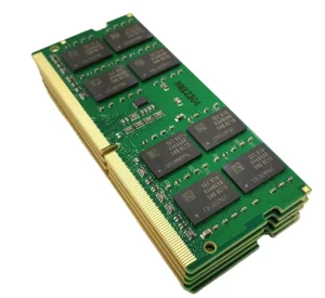
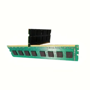
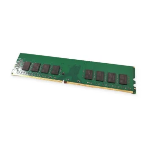
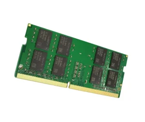
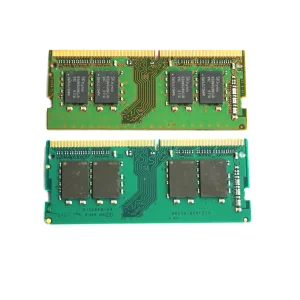
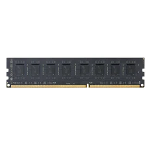
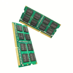
High-end computing and storage components optimized for severe temperatures and continuous operation in Nordic industrial control setups.
Technical and logistics answers for engineering and procurement professionals sourcing heavy copper PCBs for Northern Europe.
Do you have a project requiring customized Heavy Copper PCBs or PCBA engineering?
Send Inquiry Now (Get Free DFM Report)