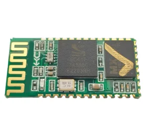
Industrial-grade circuit boards, customized flexible PCBs, and integrated memory system modules engineered for global enterprise standards.
Annual Export Value
R&D Engineers
QC Control Experts
Global Supply Chain Partners
A comprehensive deep-dive into materials science, substrate processing, and thermal dissipation metrics.
In modern electronic hardware architectures, the selection of the substrate material and layer distribution forms the bedrock of signal integrity and thermodynamic stability. Single-sided printed circuit boards represent the foundational benchmark of PCB design, consisting of a single layer of conductive copper laminated onto a rigid or flexible dielectric core. While suitable for cost-sensitive, low-frequency systems like LED arrays, basic control modules, and legacy consumer appliances, the lack of an auxiliary trace path limits their execution scope.
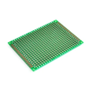
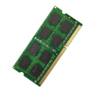
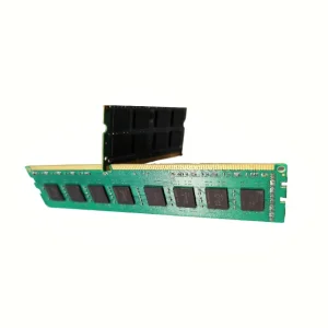
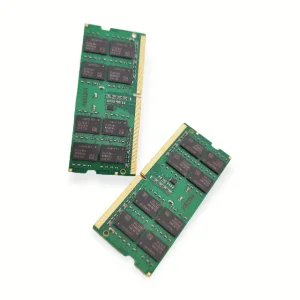
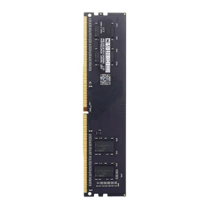
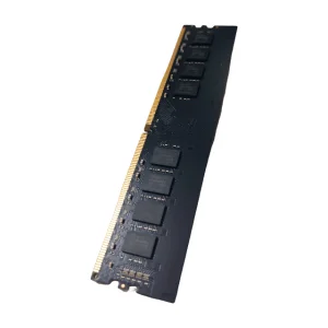
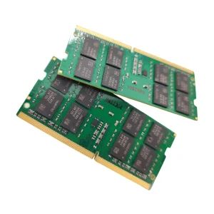
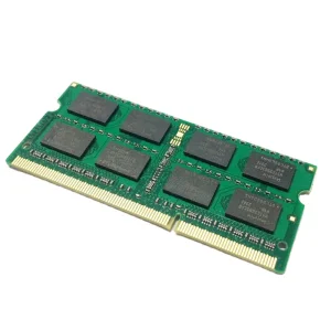
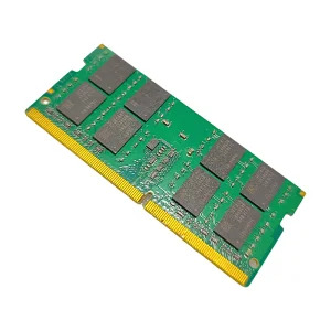
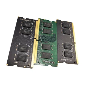
Conversely, double-sided PCBs introduce high-density routing paradigms through plated through-holes (PTH) and microvias. By utilizing both upper and lower conductive layers, design engineers can route complex matrix structures, segregate power planes from high-speed digital buses, and integrate critical shielding layers. This is essential for precision devices like memory modules, gaming computer rigs, and industrial sensor hardware. Plating double-sided systems requires extreme mechanical accuracy in drill alignment and copper deposition inside the barrel to prevent trace discontinuities.
"For modern high-speed memory systems, such as DDR4 and DDR5 modules, the underlying PCB design acts not merely as a mechanical platform, but as a transmission line system where electromagnetic propagation must be tightly controlled." — Engineering Insights Team, Vorynex Memory Technology.
Substrate materials dictates the electrical, thermal, and mechanical limits of the final PCB assembly. When sourcing Single or Double Sided PCBs, global procurement teams must audit the fundamental physical constants of the raw laminate materials. Properties such as Glass Transition Temperature (Tg), Coefficient of Thermal Expansion (CTE), and Dielectric Constant (Dk) directly govern field reliability.
| Substrate Category | Dielectric Constant (Dk) | Thermal Conductivity | Glass Transition (Tg) | Primary Application Areas |
|---|---|---|---|---|
| Standard FR-4 (Epoxy/Glass) | 4.2 - 4.8 | 0.2 - 0.4 W/m·K | 130°C - 140°C | General consumer electronics, power modules, standard RAM PCBs | High-Tg FR-4 | 4.0 - 4.5 | 0.3 - 0.5 W/m·K | 170°C - 180°C | Multi-layer systems, heavy-duty server motherboards, industrial PCs |
| Aluminum-Clad Substrate | 3.0 - 4.5 | 1.0 - 3.0 W/m·K | 130°C - 150°C | High-power LED backlights, solid-state relays, power converters |
| Taconic TLY-5 (PTFE/Fiberglass) | 2.2 | 0.22 W/m·K | 280°C+ | High-frequency RF, microwave antennas, aerospace signal buses |
As transmission bus frequencies escalate into the gigahertz realm (as seen in memory modules operating from 2133MHz to DDR5 speeds), the geometry of the traces becomes critical. Double-sided PCBs allow for the design of coplanar waveguides and microstrip routing formats, providing a clear reference plane beneath the signal tracks. This spatial configuration allows engineers to control the impedance target (typically 50 ohms for single-ended or 100 ohms for differential lines) to minimize signal reflections and maintain jitter margins.
Custom substrate engineering designed to withstand extreme thermal, electrical, and mechanical environments across industries.
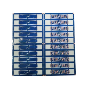
Delivering high-integrity double-sided and multilayer layouts supporting multi-channel RAM architectures (DDR4/DDR5) and dual M.2 solid-state systems. Engineered with low-loss dielectrics to withstand 24/7 server workloads.
Implementing heavy copper cladding (up to 3 oz) and robust double-sided structures for high-current applications. Ideal for power converters, electric vehicle sensor blocks, and precision metal detection sub-circuits.
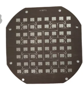
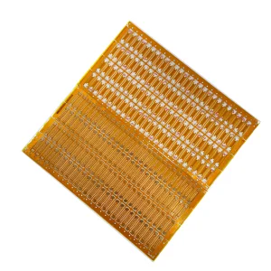
Miniaturization solutions using ultra-thin polyimide substrates and FPC technology. Featuring dense trace widths and fine spacing, perfect for complex keyboard arrays, smart displays, and compact consumer items.
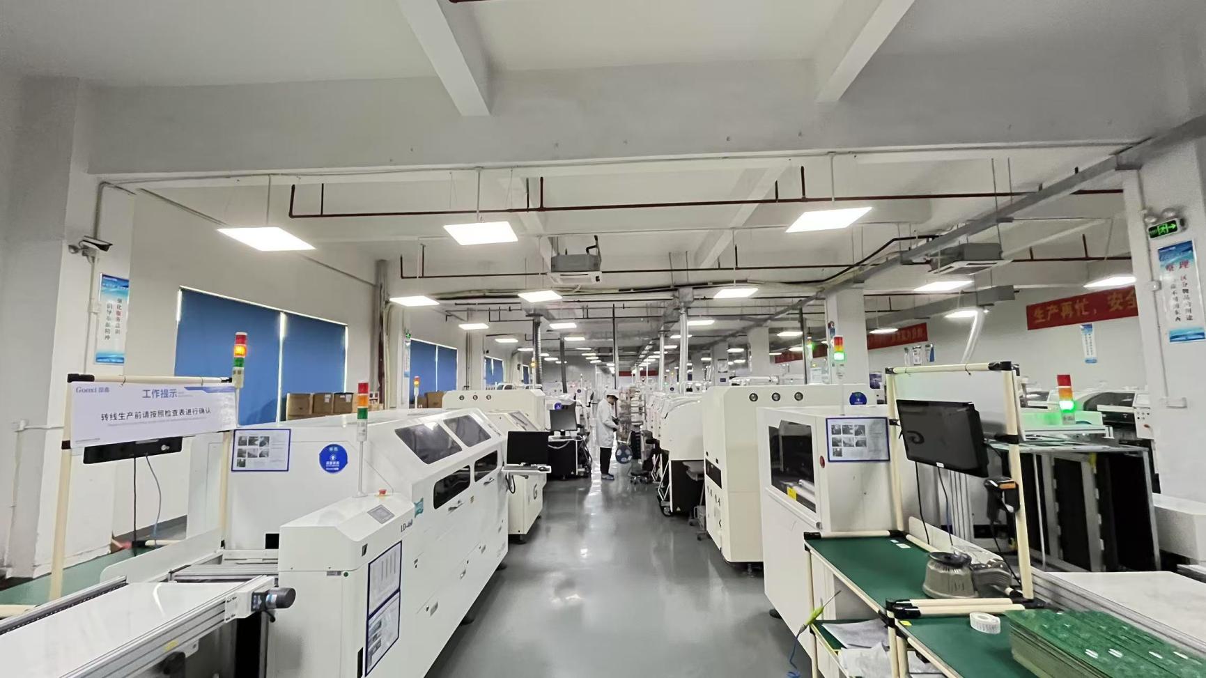
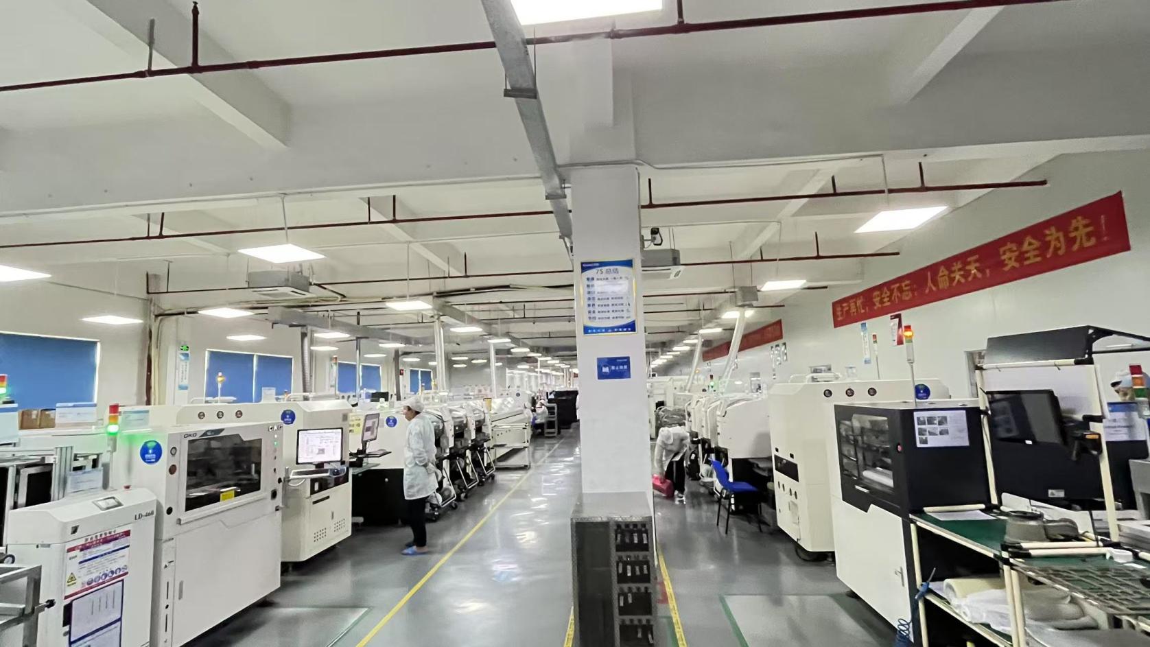
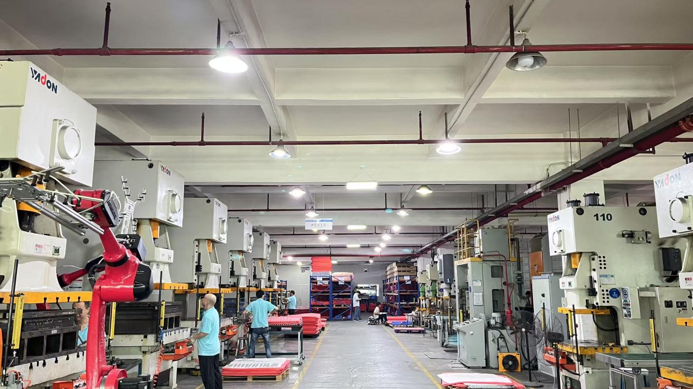
Inside Vorynex's advanced production environment, integrating SMT assembly, multi-stage testing, and material sourcing.
Vorynex Memory Technology (China) Co., Ltd., established in 2016, serves as a prominent example of China's high-tech manufacturing upgrades. Our engineering facilities utilize automated pick-and-place lines, lead-free reflow ovens, and intelligent optical sorting systems. With over 12 years of industry experience in high-precision micro-circuits and memory modules, we deliver reliable PCB configurations to markets globally.
Our quality assurance workflow utilizes a multi-layered check system to ensure zero-defect outgoing batches. We employ Automated Optical Inspection (AOI) to scan for solder joint defects, short circuits, and polarity alignments. For critical circuit traces, In-Circuit Testing (ICT) verifies component values, impedance targets, and continuous electrical paths. In addition, our 45 professional QC specialists conduct 100% functional testing, high-temperature stress testing, and real-world system compatibility checks before packaging.
Integrated Component Sourcing: Backed by a network of over 1,200 supply chain partners, we secure high-grade DRAM chips, low-loss laminate substrates, and specialized coatings. This supply chain stability protects global procurement partners from volatile raw material lead times.
Our R&D team of 180 experienced engineers works closely with clients on customized projects, covering custom PCB layout design, thermal management, heat sink modeling, frequency matching, and firmware adjustments. Within the past year, we have introduced around 240 new product designs across high-speed DDR4, next-generation DDR5, and specialized industrial PC boards.

Reliable export services with strict adherence to international electrical, mechanical, and safety standards.
All double-sided and single-sided PCB designs adhere to key global standards, including UL 94V-0 flammability ratings, RoHS environmental compliance, and CE markings. Our production methods comply with IPC-A-600 standards for rigid board quality.
With 6 years of focused export experience, Vorynex ships to key industrial centers in North America, Europe, Southeast Asia, the Middle East, and South America. We handle complex customs procedures to ensure on-time delivery.
We provide full-cycle engineering support, from initial CAD layout review to rapid prototyping and high-volume manufacturing. Custom services include private-label printing, trace optimization, and multi-chip module integration.
Answers to technical questions from engineering teams, procurement leads, and system integrators.
Explore our complete catalog of industrial RAM modules, server-grade hardware, and high-frequency printed boards.