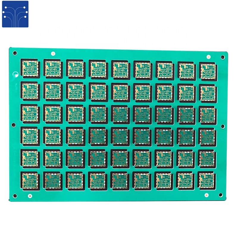
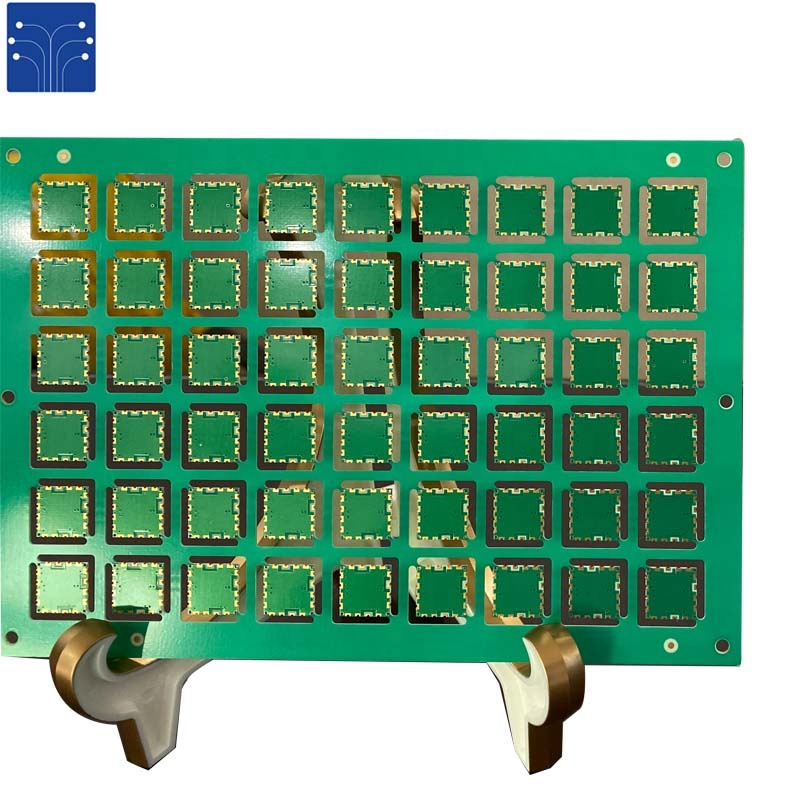
Production Capability
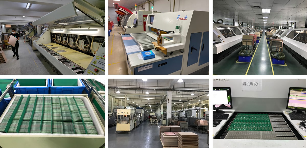
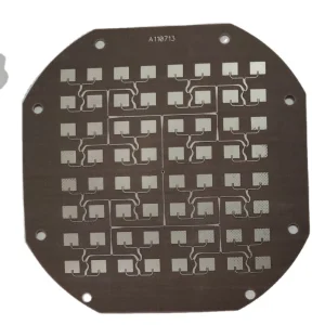
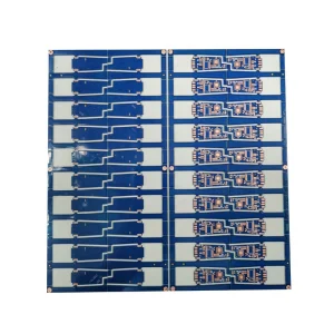
We have invested in the best equipment, environment, and staff training to ensure high-standard manufacturing operations. Our facilities deliver robust production capabilities for standard and HDI, Rigid, RF, and high-frequency PCBs. This includes through-hole configurations, min 0201 chips, and 0.2mm pitch BGA balls SMD soldering, serving small batch, mid-volume, and high-volume orders.
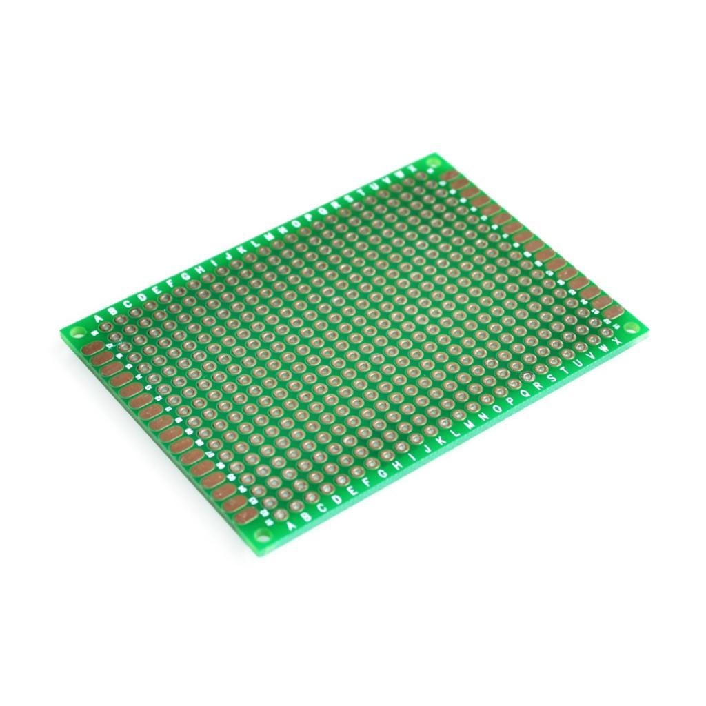
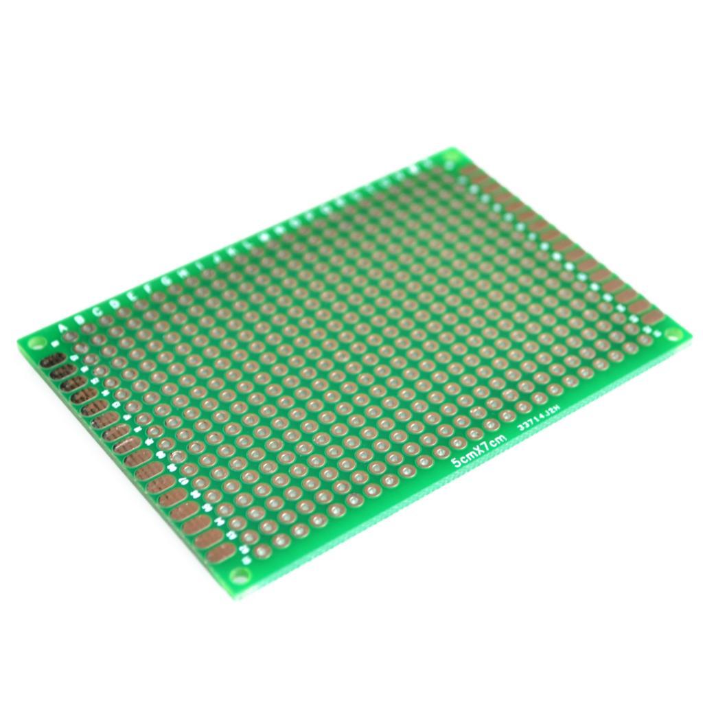
Our boards (7x9cm, 9x15cm, pack of 4, each size 2 pieces) are designed thick and double-sided. Constructed using high-grade FR4 glass fiber, they solder exceptionally well on both sides. Designed with smooth, safe edges, they are sturdy, practical, and easy to use. Pre-tinned plated holes offer a solid base, and each column and row is clearly labeled to minimize assembly errors. These boards are ideal for transferring your circuit design seamlessly from a breadboard to a permanent circuit board, making them perfect for DIY electronics and product engineering.
Highlighted Product Specification:
5*7cm Double-Sided Prototype PCB Breadboard - Printed Circuit Board Tinned Universal PCB Circuit Board (Green)
To help you evaluate our products firsthand, we are pleased to offer free samples. You only need to cover the shipping costs. Please share your delivery address and specific requirements so we can arrange your sample shipment.
| Items |
Capacity / Service Information |
| 1. Base Material |
FR4 Glass Fiber |
| 3. Copper Thickness |
1oz Copper |
| 5. Technics Characteristic |
Normal Standard |
| 6. Technical Requirement |
Normal Standard |
| Standard Lead Time |
7 - 10 Days |
| Fast Prototype Lead Time |
24 Hours ~ 72 Hours |
| Customer Service |
Should you face any issues with our products, please feel free to reach out. We provide professional, responsive pre-sales and after-sales support to assist you promptly. |
| Product Warranty |
We stand behind our products with a 100% quality guarantee. If you encounter issues or are not fully satisfied, we will provide an unconditional refund process to secure your purchase. |
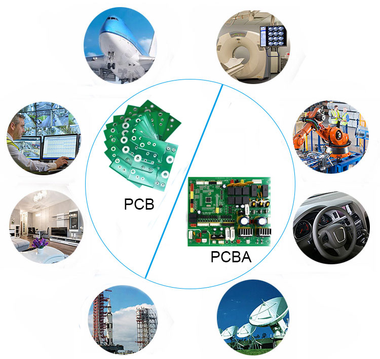
Applications and Our Services
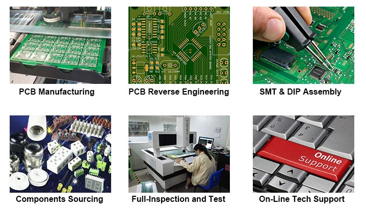
A One-Stop EMS Contract Manufacturer
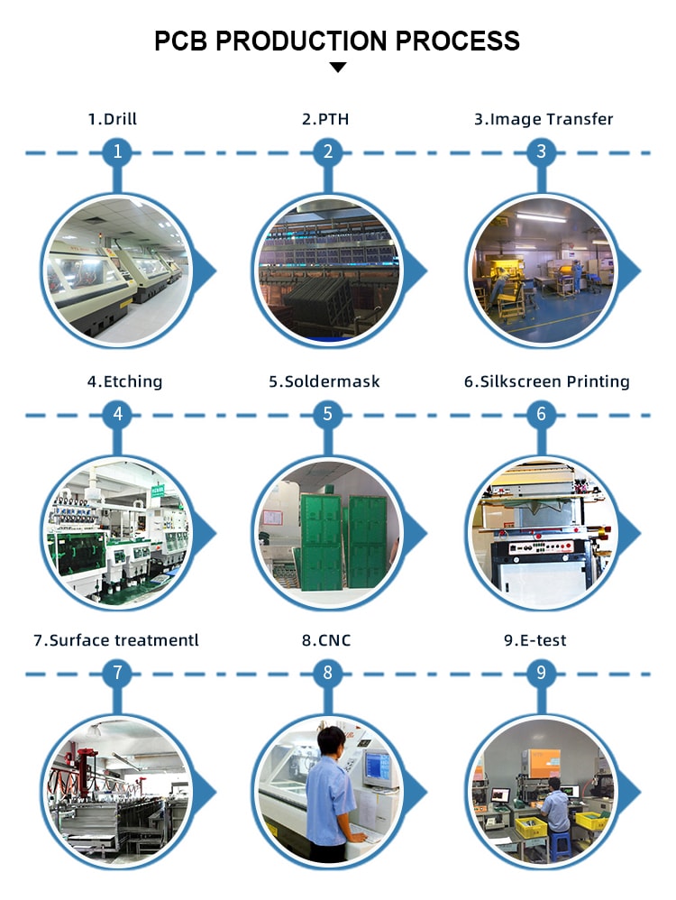
Our quality management processes are established in accordance with ISO9001 standards, strictly implementing the IPC Class III standard for all quality inspections. A 100% inspection protocol is applied, including electrical testing and automated optical inspection (AOI). We execute high-voltage testing, impedance testing, microsectioning, weldability checks, and other specialized test runs to ensure compatibility with high-tech application requirements.
Our End-to-End Capabilities:
CAM and BOM Engineering
PCB Manufacture
Materials Management
SMT and DIP Assembly
PCB and PCBA Quick-Turn Prototyping
Program and Testing
Cable Assembly Operations
Functional Board Testing
Final Enclosure & Case Assembly
Custom Packing Options
Integrated Logistics Services
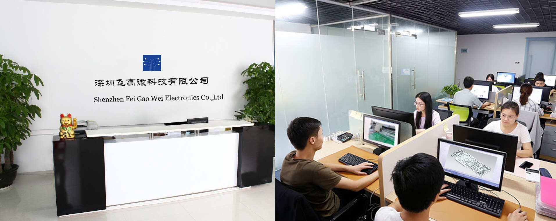
Company Introduction
We have been manufacturing high-reliability printed circuit boards for more than 20 years. Established in 1990, we serve as a globally competitive supplier specializing in high-tolerance, high-quality, and small-to-medium volume PCB production. From rapid prototype assemblies to large-scale production orders, we maintain the operational capacity and engineering expertise to fulfill all of your PCB requirements.
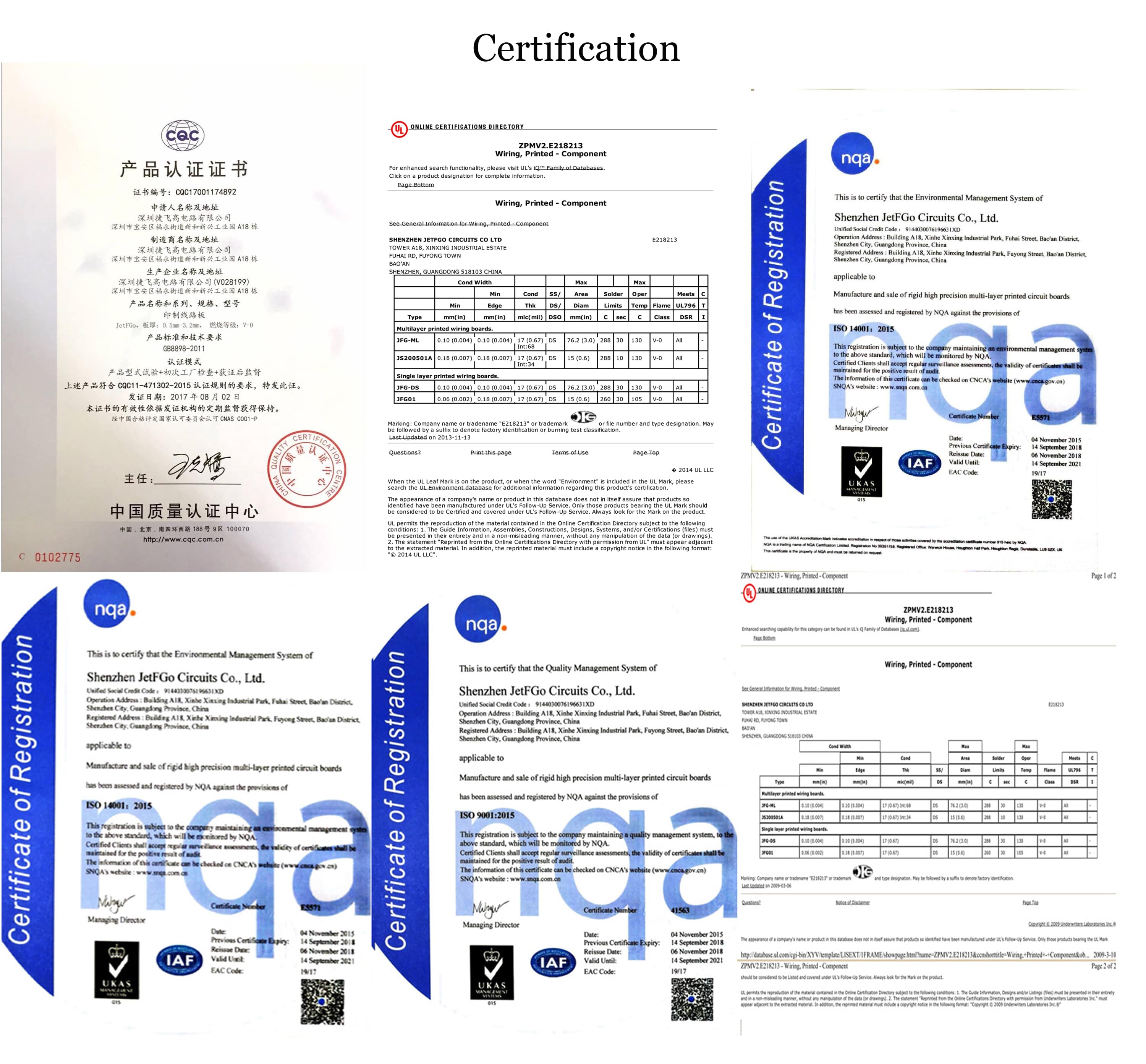
We are dedicated to offering a professional, customer-focused service where quality is paramount, fully aligned with our ISO9001 Quality Management System and UL standards.
Specializing in quick-turn services, we offer an industry-leading turnaround time of as fast as 24 hours. When your team needs rapid PCB prototyping, you can rely on us to deliver high-quality, precise boards on time and at competitive prices.
We encourage prospective clients to visit our facilities. Operating with an open-door policy for new and returning clients, we believe that reviewing our equipment and consulting with our engineering staff directly will demonstrate our capability to meet your individual specifications. We look forward to cooperating with you on your high-quality PCB projects.
Why Choose Us
We employ over 15 professional engineers, ensuring all products are fully tested and approved before inventory entry and shipment.
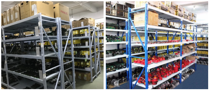
We maintain a large stock of active products. When you need to purchase or repair control system components, we are here to support your requirements.
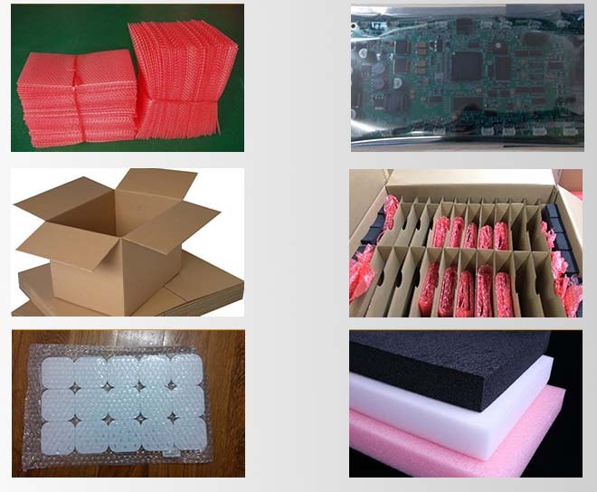
Packing & Shipping
We focus on delivering high-quality products while ensuring secure, industry-standard packaging. Personalized packing configurations are supported for all orders.
Common Packaging Methods:
• PCB: Sealed moisture barrier packaging, anti-static bags, and custom-fit protective shipping cartons.
• PCBA: Protective ESD foam cushioning, anti-static shielding bags, and robust external cartons.
Customized Shipping Cartons:
Outer cartons can be custom printed with details such as client branding, shipping marks, destination data, and other specifications as requested.
OEM/ODM Services
We offer comprehensive, one-stop PCB/PCBA customization services, aiming to meet all specifications requested by our customers. To guarantee top-tier board quality, we perform extensive quality validation procedures prior to shipping:
Outgoing Testing: Verification of min PTH Cu thickness, surface Cu thickness, ENIG Au/Ni thickness data, gold layer adhesion, solder mask adhesion, silkscreen adhesion, thermal stress, hardness, twist, and bow tolerances.
Microsection Evaluation: Inspection of inner-hole copper thickness, surface copper thickness, wrap copper structure, hole wall integrity, solder mask thickness, and stack-up details.
Electrical Testing: 100% E-test checks for any open or short circuits.
Thermal Stress Testing: Run to eliminate risks of delamination, measling, or laminate voiding.
Solderability of PTH: Checks to prevent discoloration, wrinkling, blisters, blow-holes, solder mask peeling, or incomplete solder mask fills inside hole walls. Impedance testing is performed according to specifications.
Please contact us to discuss your design requirements.
Frequently Asked Questions
How do you guarantee the quality of the components?
We provide a 3-month warranty for used parts and a 1-year warranty for brand-new components. If you receive a component that does not perform correctly, you can return it within 7 days, and we will cover return shipping costs.
What packaging standards do you use for shipping?
We utilize 3cm thick foam board lining inside our cartons to protect components from transit shock. Heavy parts are packed in customized wooden crates for maximum protection.
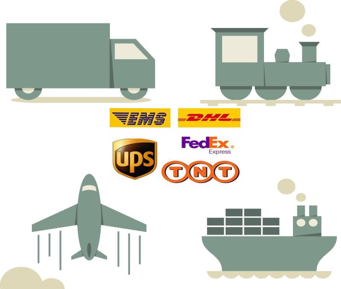
Which payment methods and express shipping options do you support?
We accept standard payment methods including T/T (Bank Transfer), PayPal, Western Union, Secure Platforms, etc. For shipping, we work with primary express carriers such as DHL, FEDEX, UPS, TNT, and EMS.
Do you test parts before shipment and what is your lead time?
Yes, we maintain testing equipment and 100% of our products undergo functional verification before shipping. For stocked parts, order dispatch typically takes 1 to 2 business days.
Can you manufacture boards from a physical PCB sample if I do not have Gerber files?
Yes, we can reverse-engineer a Gerber design file from your physical sample. Production runs are then executed based on the generated file. We can also develop Gerber files from schematic diagrams supplied by our clients.
Are my proprietary design files kept secure?
Absolutely. All customer design documentation and Gerber data are kept strictly confidential within our factory operations. We do not share intellectual property with third parties and are pleased to sign a Non-Disclosure Agreement (NDA).