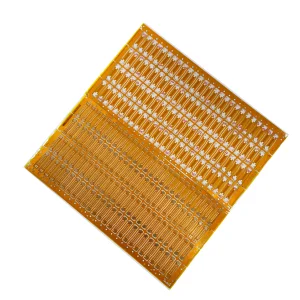
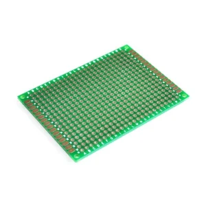
High-precision double and single-sided printed circuit board products optimized for smart sensing, telecommunication infrastructure, and IoT hardware.
The Greater Paris region (Île-de-France) stands as a prominent nexus for European research and development, smart mobility networks, and hardware innovations. Key technological nodes such as the Paris-Saclay cluster drive unprecedented demands for high-quality electronics components. In this environment, double-sided and single-sided printed circuit boards are fundamental building blocks. Standard requirements focus on robust dielectric constants, high thermal management, and low trace tolerances.
Local French hardware integrators, robotics startups, and smart city infrastructure agencies face a delicate balance: sourcing components that meet strict European Union quality regulations (CE, RoHS, REACH) while containing costs to preserve design agility. Our factory steps in as a direct-to-market partner, combining state-of-the-art Chinese manufacturing efficiencies with high-level technical expertise to deliver reliable boards to Parisian companies.
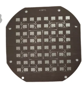
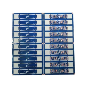
As smart urban infrastructure expands—ranging from electric vehicle (EV) fleet charging stations along the Seine to energy grid control cabinets—electronic design relies heavily on thermal dissipation, component footprint reduction, and circuit durability. Our range of single-sided copper clad laminates and double-sided plated-through-hole (PTH) PCBs meet these requirements, ensuring stable long-term performance under demanding operating environments.

An engineering deep-dive on design parameter validation, substrate options, thermal control mechanics, and quality assurance processes.
We process standard FR-4, CEM-1, Polyimide flex materials, and thermal-dielectric aluminum cores. For high-frequency microwave applications, we supply specialty laminates such as Taconic TLY-5 (0.254mm thickness), delivering low loss tangent values and exceptional dimensional stability.
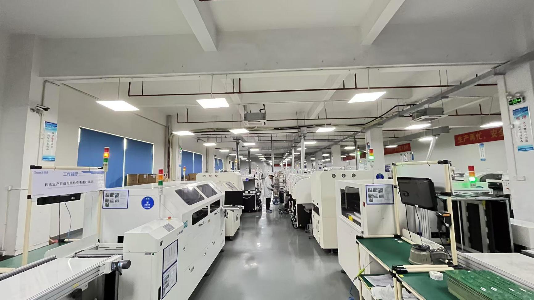
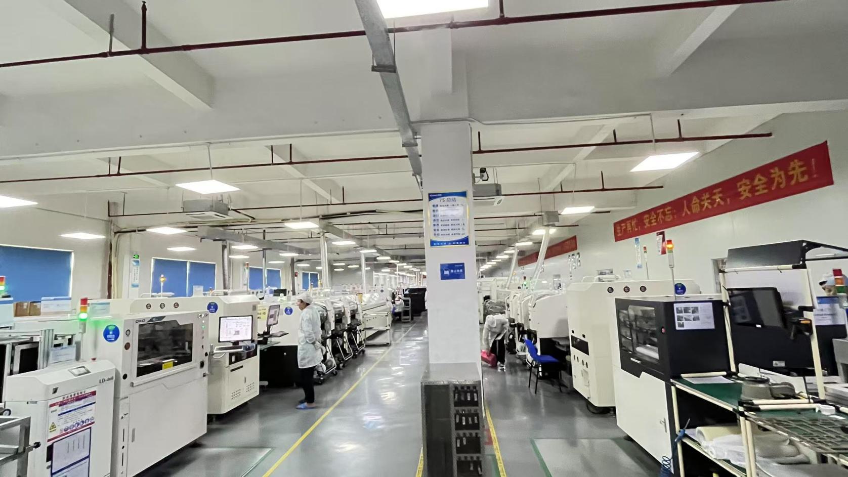
Our quality control protocol incorporates Automatic Optical Inspection (AOI), In-Circuit Testing (ICT), and system-level validation. With 45 dedicated quality control professionals, we ensure that trace geometry, layer registration, and through-hole plating comply with strict industry standards.
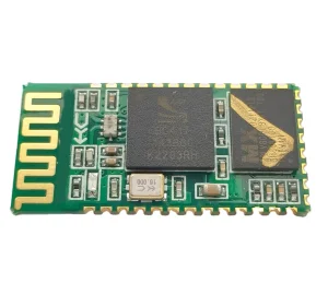
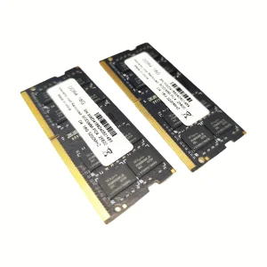
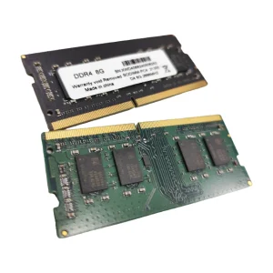
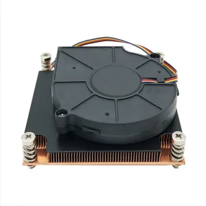
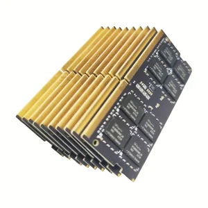
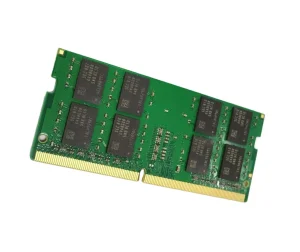
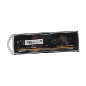
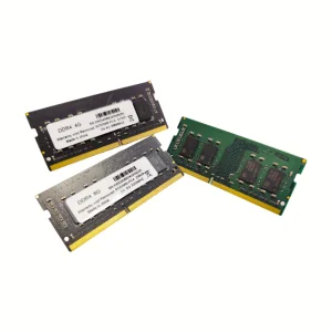
Our capabilities bridge custom PCB designs and specialized electronics. This includes high-sensitivity metal detector boards, flexible polyimide HMI membranes, server thermal solutions, and premium DRAM modules tailored for enterprise applications.
Vorynex Memory Technology (China) Co., Ltd. - Specialized design, engineering, and manufacturing capabilities.
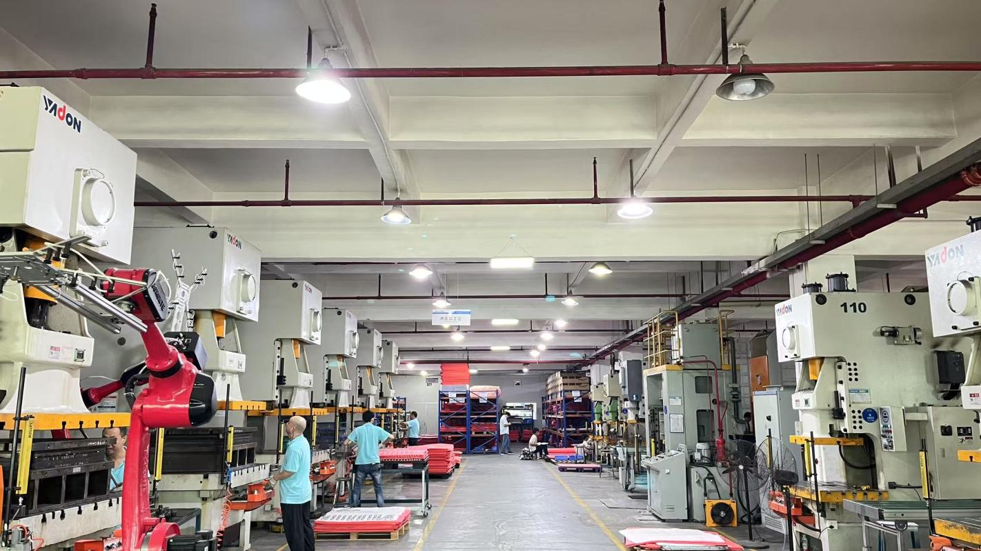
Established in 2016, Vorynex has developed strong manufacturing and engineering capabilities over the years. With a specialized and modern high-precision fabrication cleanroom facility covering approximately 320㎡, Vorynex focuses on delivering stable, high-speed, and energy-efficient memory systems and printed circuit board assemblies for gaming, industrial, and enterprise applications.
Supported by 6 years of export experience and over 12 years of industry experience in high-precision circuits, PCB fabrication, and memory architecture fields, our annual export revenue has reached approximately USD 12 million. We maintain strict quality control standards, including 100% functional testing, aging tests, compatibility testing, and high-temperature stress testing.
We collaborate with more than 1,200 supply chain partners, enabling stable sourcing of high-quality DRAM chips, base copper laminates, and electronic components. Our dynamic team of 180 R&D engineers continuously refines routing design, signal integrity, and thermal performance, introducing approximately 240 new custom models annually.
By routing design schematics directly to our advanced manufacturing lines, we bypass typical intermediary bottlenecks, ensuring fast delivery to the French market. Our Industry 4.0 integration links component sourcing, smart routing machines, and robotic pick-and-place lines. This reduces human error and maintains trace width integrity down to +/- 0.05mm.
This systematic level of integration is essential for double-sided PCBs, where inner-layer connectivity and plated-through-hole (PTH) reliability are critical. Using premium electrolytic copper baths and automated plating monitors, our production lines achieve uniform wall thickness inside micro-vias, resolving a common failure point in high-vibration automotive or sensor systems.
Additionally, our logistics partnerships enable seamless shipping options. Whether sending fast air-freight prototypes to Paris-Charles de Gaulle (CDG) Airport or high-volume sea cargo containers, we coordinate custom clearing documentation to streamline the import process for European buyers.
How smart electronics solutions fit into Parisian technology, transit, and computing infrastructure.
Fitted with high-frequency RF dielectric PCBs, specialized copper heat sinks, and server-grade memory modules, our products support continuous data processing demands in the Seine-Saint-Denis cloud hubs.
Single and double-sided boards form the backbone of vehicle tracking nodes, automated transit gates, and environmental monitoring networks across Paris.
High-sensitivity detector circuits and PCBA setups provide long-term reliability for security systems, automation, and metal detection machinery.
OEM components, prototype boards, heat dissipation hardware, and memory systems optimized for enterprise technology deployments in Paris.
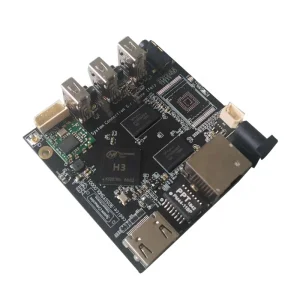
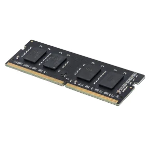
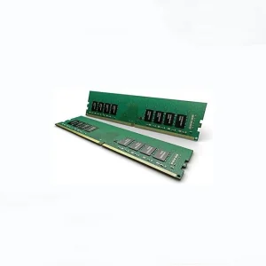
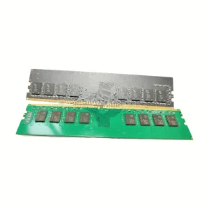
Extended hardware modules and system components optimized for high-speed computing setups.
Detailed engineering and logistical insights for procurement managers in Paris and the EU.
Our rapid prototyping services deliver complete single or double-sided PCBs within 3 to 5 business days, followed by 2 to 3 days for express air courier delivery to Paris. Standard high-volume production orders typically complete within 10 to 15 business days, depending on BOM complexity and testing requirements.
We source raw materials and laminates that comply with EU RoHS directive 2011/65/EU and REACH regulations. All board surface finishes, including Lead-Free HASL, ENIG, and OSP, are certified lead-free. Fully compliant documentation and safety sheets are provided with every shipment.
Yes, we maintain partnerships with specialized material suppliers, allowing us to fabricate circuits using Taconic TLY-5 (0.254mm thickness), Rogers series laminates, and high-Tg FR-4. These materials are suitable for radar modules, aerospace telemetry, and high-frequency communication antennas.
Every batch undergoes Automated Optical Inspection (AOI) to verify trace continuity and geometry. Additionally, we conduct In-Circuit Testing (ICT), high-temperature stress tests, and final system validation. Our team of 45 QA technicians performs visual checks under microscope systems to confirm solder mask integrity and plated-through-hole quality.
Yes, we provide full turnkey PCB assembly services. This includes sourcing electronic components, fabricating the boards, SMT pick-and-place placement, reflow soldering, hand assembly for through-hole parts, programming, and functional testing.
Optimize your hardware development timeline and improve supply chain reliability. Submit your Gerber files and BOM to our engineering desk for a comprehensive quote.
Send Inquiry Now