Featured electronics designed to control precision UV emission arrays, integrate edge computing in sterilization chambers, and run automation nodes for Boston research facilities.
The optoelectronics industry has undergone a monumental shift toward solid-state lighting, and the UV spectrum is no exception. The 3535 surface-mount device (SMD) packaging—measuring 3.5mm by 3.5mm—has emerged as the universal standard for driving high-power ultraviolet light emitting diodes (UV LEDs). Spanning from the deep UVC range (270nm-280nm) up through UVB (280nm-315nm) and into UVA (315nm-410nm), these compact chips deliver precise, high-radiant flux output necessary for challenging physical and chemical reactions.
Operating within this range requires highly specialized manufacturing substrates. Because deep ultraviolet light degrades standard packaging epoxies, high-reliability 3535 packages utilize premium ceramic bases (such as Aluminum Nitride, AlN) coupled with quartz glass lenses to optimize transmission and withstand intensive photon energy over operating lifetimes exceeding 20,000 hours.
| Wavelength Band | Primary Physical Interaction | Target Boston Application Sector |
|---|---|---|
| 270nm - 280nm (UVC) | DNA/RNA absorption peak; induces thymine dimers preventing replication. | Pharmaceutical cleanrooms, clinical water purification, air sterilization. |
| 280nm - 315nm (UVB) | Vitamin D synthesis, plant photochemical pathway stimulation, chromatography. | Biomedical analytics, phototherapy devices, agricultural greenhouses. |
| 315nm - 400nm (UVA) | Excitation of photoinitiators for rapid radical polymerization. | High-speed industrial printing, additive manufacturing (3D printing), PCB solder mask curing. |
| 400nm - 410nm (Near-UV) | Surface chemical curing, fluorescent inspection excitation. | Non-destructive medical diagnostics, industrial epoxy curing systems. |
How the Greater Boston Area utilizes precision UV systems across academia, clinical laboratories, and advanced manufacturing.
Boston's Kendall Square and Route 128 corridor demand cleanroom sterility of the highest tier. 270nm-280nm UVC LEDs are integrated directly into biological safety cabinets, microfluidic lab-on-a-chip diagnostic kits, and high-throughput screening wells to guarantee baseline pathogen decontamination without chemical residue.
New England industrial facilities, biotech plants, and local municipal water suppliers utilize heavy-duty UVC disinfection arrays to treat process water. Eliminating heat and chemicals protects delicate analytical processes and prevents biological fouling in ultra-pure water loops.
The thriving hardware prototyping ecosystem in Boston employs 365nm to 405nm UV LEDs in advanced SLA/DLP 3D printers and industrial glue dispensers. Rapid curing cycle times are essential to sustain local R&D iteration velocities.
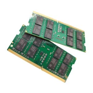
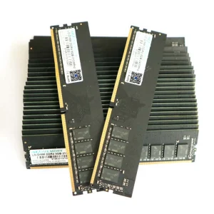
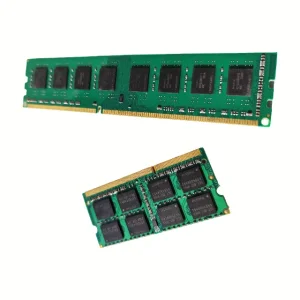
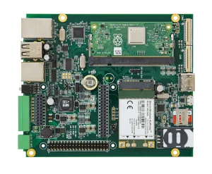
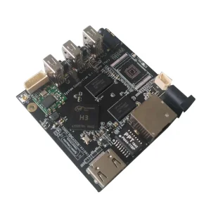
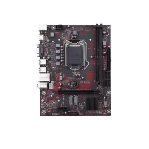
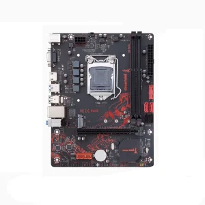
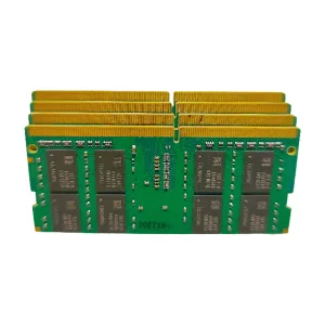
Reliable computing modules, logic boards, and thermal dissipation systems built to control active UV optical arrays.
Procuring optoelectronic components on a global scale requires strict alignment between technical parameters and delivery schedules. Global procurement managers searching for 270nm-410nm 3535 UVC LED manufacturers look beyond chip metrics; they evaluate thermal resistance, binning consistency, driving electronics compatibility, and bulk price stability. Finding a manufacturing partner who balances engineering support with volume scale is paramount.
This is where the paradigm of China Factory 4.0 steps in to bridge the gap. Industry leaders like Vorynex Memory Technology (China) Co., Ltd. serve as key examples of high-tech manufacturing capacity. Established in 2016, Vorynex has successfully integrated automated cleanrooms, precision chip mounting, and intensive electronic component assembly to serve demanding markets worldwide.
Annual Export Value
Professional R&D Engineers
QC Control Specialists
Supply Chain Partners
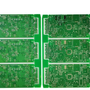
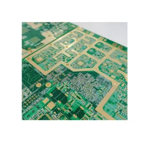
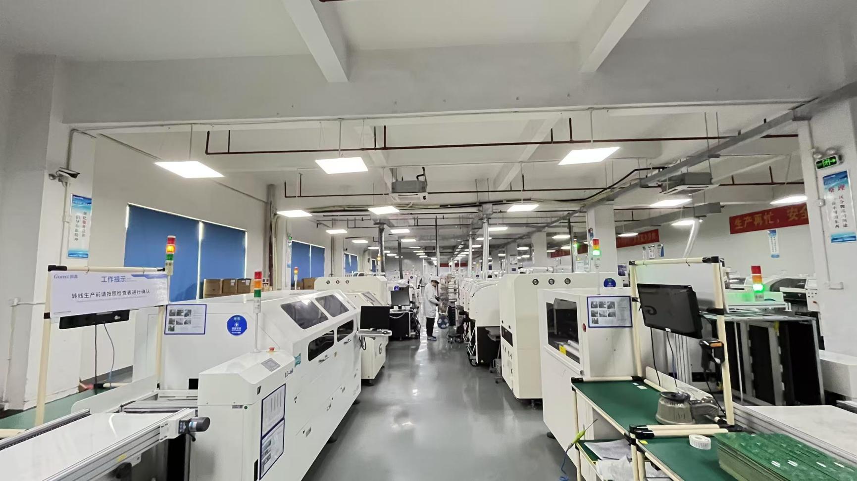
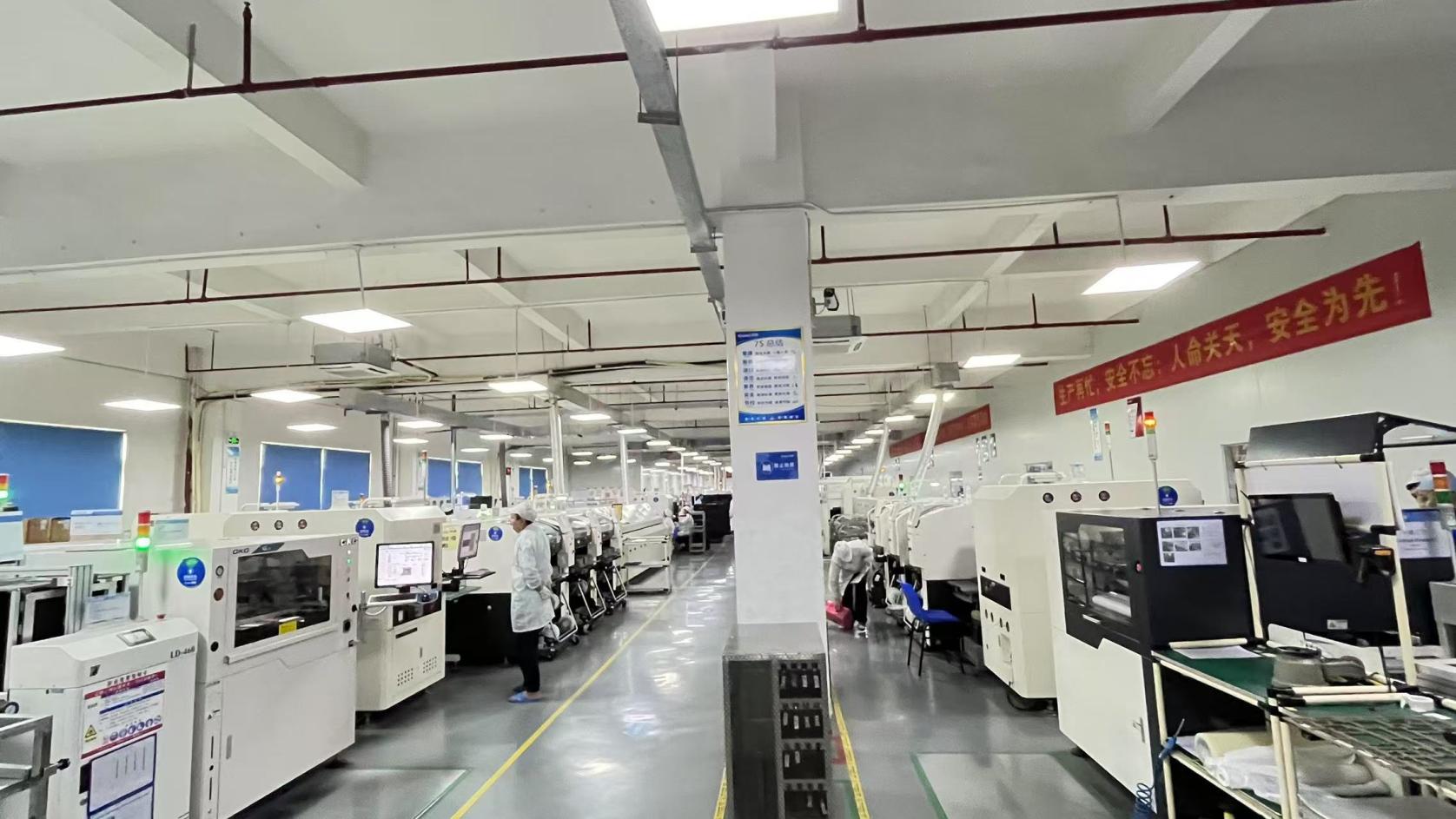
Operating a facility specialized in high-performance electronics assembly, Vorynex maintains strict, military-grade testing operations, including 100% functional testing, thermal stress verification, aging tests, and advanced automated optical inspection (AOI). By using state-of-the-art SMT lines, advanced chip-on-board (COB) capabilities, and robust supply chains, manufacturers are capable of producing stabilized UV drivers, custom PCBA modules, and specialized optical instrumentation components with minimal latency.
We support extensive customization pathways to align with complex Boston lab projects and industrial standards. Our production lines facilitate:

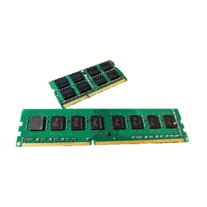
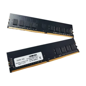
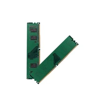
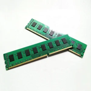
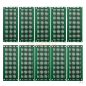
Explore our deep catalog of controller boards, industrial-grade memory, and high-frequency PCBs suitable for integration into professional UV curing machines and bioreactor automation loops.

Integrating 270nm-410nm 3535 UVC/UVA LEDs into enterprise-grade systems demands answers to complex thermal, optical, and operational inquiries. Below are key concepts addressed by our R&D engineers to ensure robust integration within Boston's regulatory and commercial frameworks.
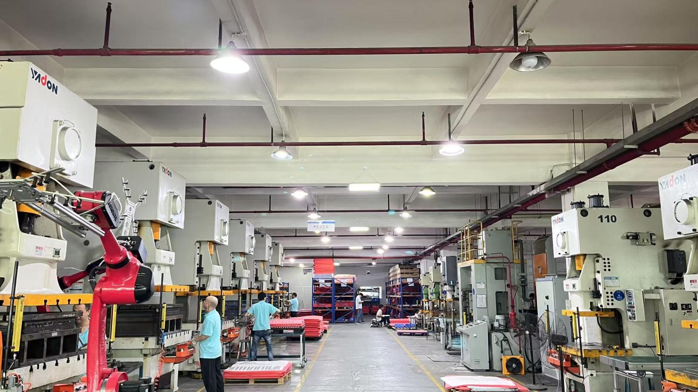
Our advanced cleanroom environment ensures particles do not compromise the integrity of high-power optoelectronic SMT and chip-mounting processes.