In high-density electronics manufacturing, procurement decisions require balancing structural integrity, thermal dissipation, signal integrity, and supply chain continuity. Let's analyze how to assess tier-1 EMS providers based on technical execution.
Evaluation of manufacturing capability begins with SMT placement density. Modern consumer and industrial systems require fine-pitch placement down to 01005 passives and micro-BGA components with pitch clearances under 0.3mm. Utilizing advanced solder paste printers, dual-lane reflow ovens, and precise pick-and-place systems prevents structural bridge failures and cold solder joints.
Power electronics and server-class motherboards run under harsh thermal conditions. Sourcing top-tier assembly ensures expert processing of high-TG substrates (TG170+), aluminum-clad PCBs, and heavy copper layers. This prevents delamination under thermal shock and ensures efficient dissipation pathways in compact enclosures.
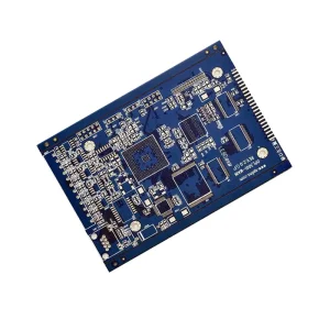
Reliability requires robust automated testing pipelines. Reliable assembly partners execute multi-stage optical and electrical testing, integrating Automated Optical Inspection (AOI) after both solder-paste print and post-reflow, In-Circuit Testing (ICT), and functional system-level validation to keep return-to-origin rates under 150 DPPM.
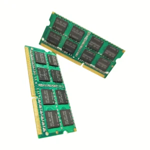
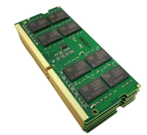
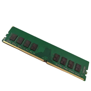
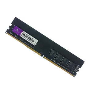
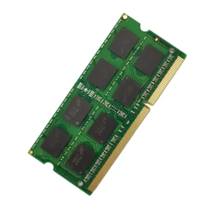
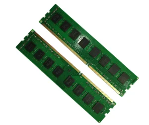
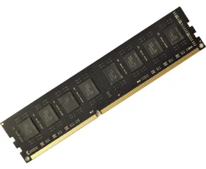
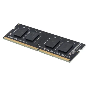
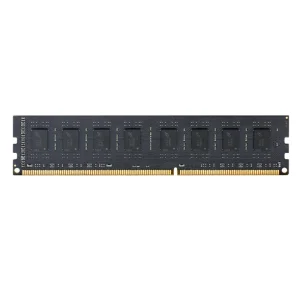
Established in 2016, Vorynex Memory Technology has developed strong manufacturing and engineering capabilities, specializing in high-performance memory modules for global markets. Operating a precision-focused manufacturing facility covering approximately 320㎡, Vorynex focuses on delivering stable, high-speed, and energy-efficient memory solutions for gaming, industrial, and enterprise applications.
With an annual export revenue of approximately USD 12 million, supported by 6 years of export experience and over 12 years of industry experience in semiconductor and memory-related fields, Vorynex maintains strict quality control standards. This includes 100% functional testing, aging tests, compatibility testing, and high-temperature stress testing.
The company collaborates with more than 1,200 supply chain partners, enabling stable sourcing of high-quality DRAM chips and components for its primary customer base, which includes brand distributors, system integrators, industrial equipment manufacturers, and gaming hardware companies.
Vorynex successfully launched around 240 new product models in the past year, showcasing their active engineering pipeline.
The electronics assembly landscape is shifting from traditional manual setup stages to highly integrated, software-driven automated assembly. Key transitions in packaging technology demand significant upgrades from global contract manufacturers.
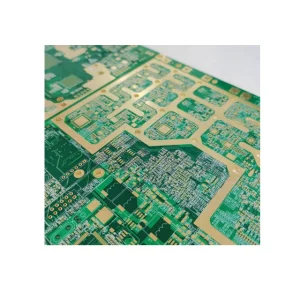
As DDR5 and PCIe Gen 5/6 become mainstream, signal loss and transmission line crosstalk become more critical. Leading contract manufacturers must implement controlled impedance micro-routing, customized via structures, and high-frequency substrates such as Rogers or Shengyi High-TG FR4 to minimize attenuation at frequencies above 10 GHz.
Mobile processors and high-performance system-on-chips (SoCs) utilize micro-BGA footprints with pitch spacing down to 0.3mm. In modern SMT environments, underfill dispensing is required to cushion the thermal expansion mismatch between silicon chips and epoxy glass PCBs, preventing mechanical solder-ball shear under stress.
Sustainability is no longer optional. The industry is moving from standard leaded assembly towards full RoHS compliance, incorporating lead-free reflow profile optimizations, halogen-free epoxy matrices, and energy-efficient nitrogen reflow systems to lower the carbon footprint of assembly operations.
Electronics assembly is not one-size-fits-all. Different industries require customized component selection and testing standards to perform under various environment conditions.
| Vertical Market Sector | Critical Assembly Standard | Predominant PCB Technology | Key Reliability Test Method |
|---|---|---|---|
| Enterprise Servers & Datacenters | IPC-A-610 Class 3 (High-Reliability) | Multi-layer (16+ layers) Backplanes, High-TG FR4 | High-Temperature Operating Life (HTOL), Thermal Shock |
| Automotive Electronics (ADAS & EV) | IATF 16949 / AEC-Q100 Components | Heavy Copper PCBs, Metal Core PCBs (MCPCB) | Power Temperature Cycling (PTC), Vibration Testing |
| Industrial Process Control & IoT | IPC-A-610 Class 2 | Rigid-Flex Boards, Conformal Coating Applied | Highly Accelerated Life Testing (HALT), Salt Spray Test |
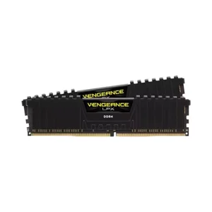
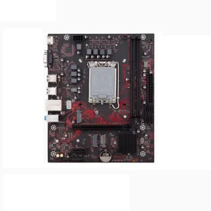
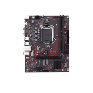
| Consumer Hardware & Gaming | IPC-A-610 Class 1 / Class 2 | Standard Double-sided FR4, High-Speed DDR4/DDR5 Slots | Compatibility Matrix Validation, Functional Benchmark Testing |
The electronics manufacturing ecosystem in China has evolved beyond simple cost efficiency into a highly integrated, automated smart manufacturing powerhouse. Through Factory 4.0 principles, modern SMT lines leverage IoT sensors, automated materials transport (AMRs), and smart ERP platforms to deliver consistent quality and scale.
By cluster-sourcing passives, active chips, and custom substrates within localized industrial hubs, assembly factories minimize transit risks. Access to over 1,200 supply chain partners ensures Vorynex and other leading manufacturers can secure raw components even during tight global shortages, mitigating lead time spikes.
Traceability is key for industrial and medical clients. China Factory 4.0 integrates 2D matrix laser marking on every PCB, tracking every solder joint, reflow temperature curve, and component lot code. In the event of a field failure, root-cause analysis is completed in hours rather than weeks.
Modular setup tools allow lines to switch from high-volume memory runs to small-batch industrial motherboards with minimal downtime. The integration of 3D solder paste inspection (SPI) and software-controlled pick-and-place placement optimizes yield rates from the very first panel.
Navigating global trade require adherence to regional regulations and standard compliance certifications. Sourcing globally requires choosing partners who maintain verified quality systems.
All materials—including laminate resins, copper foil, component packages, solder alloys, and cleaning agents—must be verified lead-free and free of Restricted Hazardous Substances (RoHS). Compliance ensures smooth customs clearance at EU and North American ports, protecting system integrators from regulatory liabilities.
For mission-critical hardware (medical monitors, server storage arrays, avionics), the IPC-A-610 Class 3 standard ensures zero tolerance for solder voids, component misalignment, or trace damage. Modern SMT factories maintain dedicated certified IPC trainers on-site to inspect high-density joints.
Key industry answers for procurement officers and system engineers seeking assembly partners.
For prototype builds, assembly takes 3 to 7 working days once all parts are received. For mass production runs (e.g., 5,000+ units), typical lead times range from 4 to 6 weeks, which includes component sourcing, bare board fabrication, SMT placement, testing, and final packaging.
Vorynex utilizes a multi-step verification process: First, 100% automated optical inspection (AOI) detects component misalignment. Second, in-circuit testing (ICT) verifies capacitor and resistor tolerances. Finally, the modules undergo motherboard validation across major platforms (Intel, AMD) under high-temperature stress tests to verify real-world SPD profiles and data transmission rates.
HASL (Hot Air Solder Leveling) is cost-effective and suitable for standard component mounting, but leaves a slightly uneven surface. ENIG (Electroless Nickel Immersion Gold) provides a flat surface finish, ideal for fine-pitch BGA arrays and high-density packaging, and offers superior shelf life and resistance to environmental oxidation.
Without careful impedance control, high-frequency signals experience reflections and phase shifts, leading to data corruption and system crashes. Manufacturers use specialized design tools and real-time coupon testing to maintain impedance tolerances within +/- 10% (typically 50 ohm single-ended, 90 or 100 ohm differential).
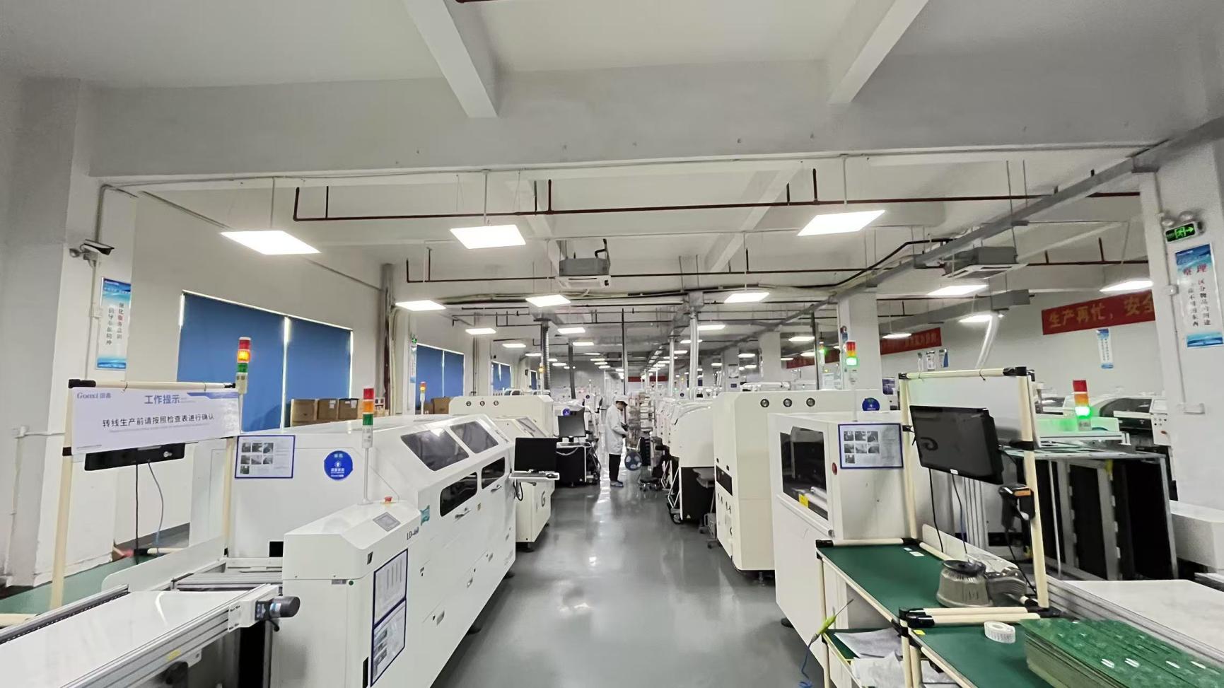
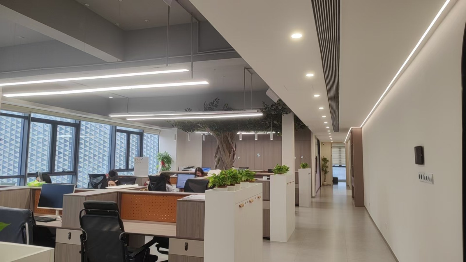
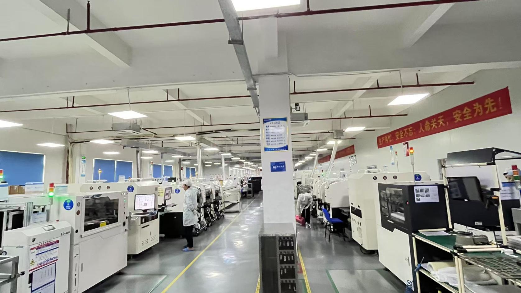
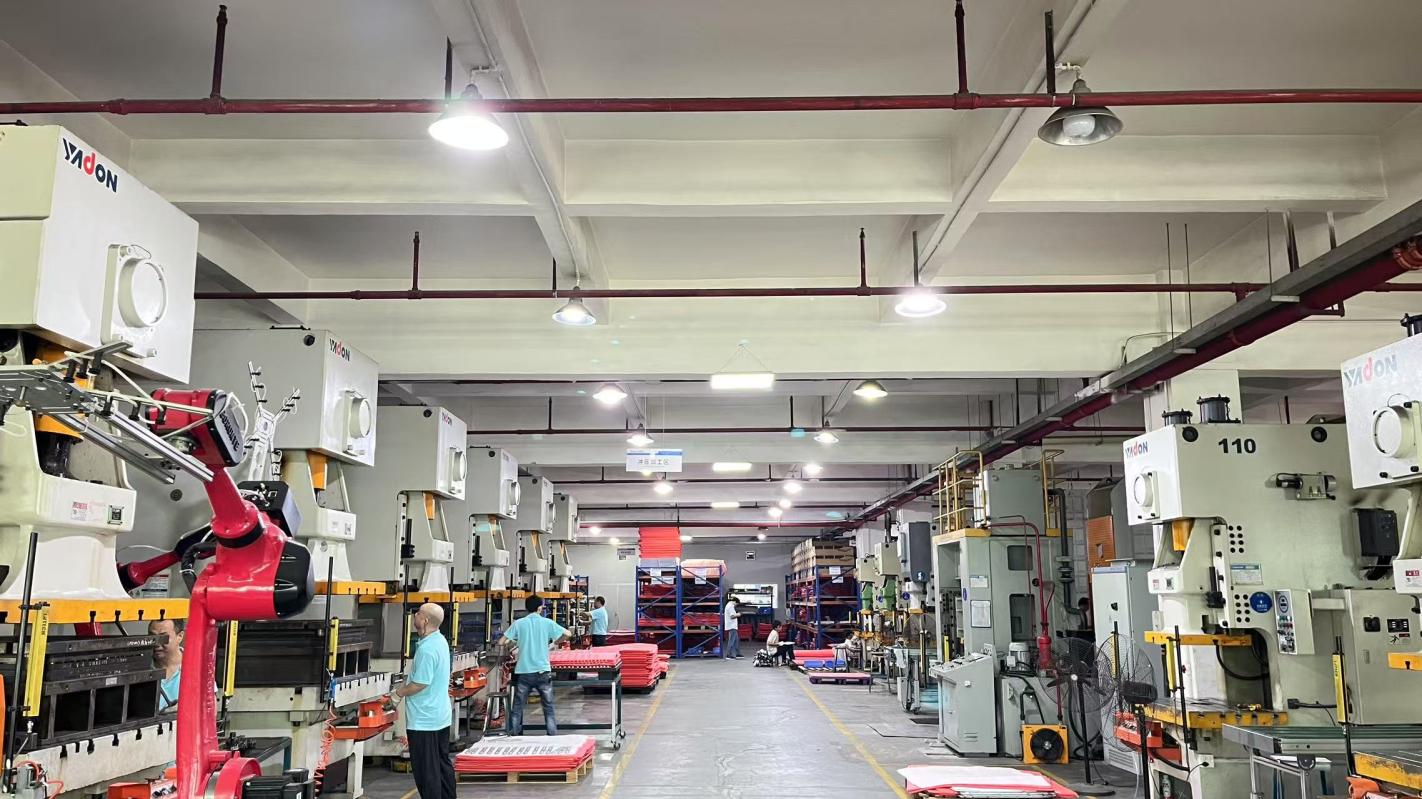
Take a visual tour of our cleanroom facilities, testing platforms, and modern warehouse storage areas built to support high-density semiconductor processing.