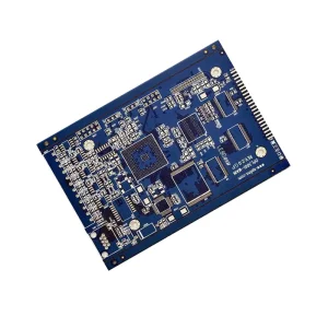
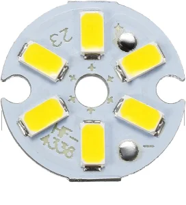
Engineered to meet the absolute reliability standards of the Chubu region's heavy industries, featuring advanced thermal substrates, multi-layer designs, and rigorous qualification protocols.
Nagoya, located in the heart of Japan's Chubu region (Aichi Prefecture), represents the absolute pinnacle of global industrial manufacturing. Famed for its deep-rooted philosophy of Monozukuri (the art, science, and state-of-mind of making things), this economic powerhouse drives the global automotive, aerospace, machine tools, and industrial robotics sectors. From the sprawling assembly plants of Toyota and Mitsubishi Heavy Industries to the cutting-edge labs designing Next-Gen eVTOL (electric vertical takeoff and landing) aircraft, Nagoya demands electronic hardware of uncompromising quality, high-temperature resilience, and flawless signal integrity.
Industrial environments in Nagoya are notoriously challenging for electronic assemblies. High vibrations in robotic joints, extreme thermal cycling in automotive engine bays, and EMI (electromagnetic interference) challenges in high-voltage EV platforms mean that off-the-shelf printed circuit boards often fall short. Modern systems require PCBs designed with high Glass Transition Temperatures (Tg > 170°C), precise characteristic impedance control, and advanced surface finishes like Immersion Silver or ENIG (Electroless Nickel Immersion Gold) to ensure long-term, oxidation-free connectivity in humid coastal microclimates.
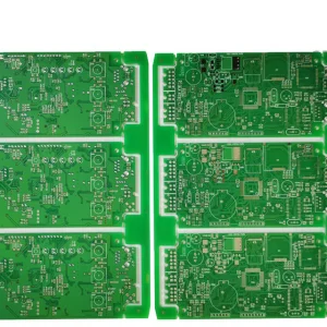
As a major exporter serving this elite market, Vorynex Memory Technology (China) Co., Ltd. integrates state-of-the-art Chinese manufacturing efficiencies with custom engineering protocols designed specifically to cross-reference and align with Japanese JIS standards. We supply multi-layer boards, HDI circuits, power supply PCBA assemblies, and specialized memory solutions that ensure flawless operations within Nagoya's industrial computing architectures.
In the current semiconductor landscape, global enterprises are balancing the need for rapid speed-to-market with rigorous cost control. The Shenzhen-Dongguan-Guangzhou electronics cluster in China represents the most comprehensive PCB supply chain ecosystem in the world. By outsourcing production to Vorynex, Nagoya enterprises secure several vital advantages:
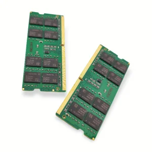
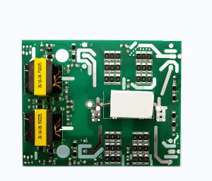
Heavy-duty control boards, LED systems, and computing motherboards tailored for industrial display, processing, and heavy welding machinery in the Tokai region.
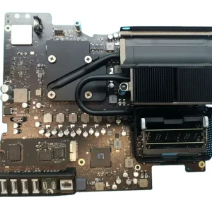
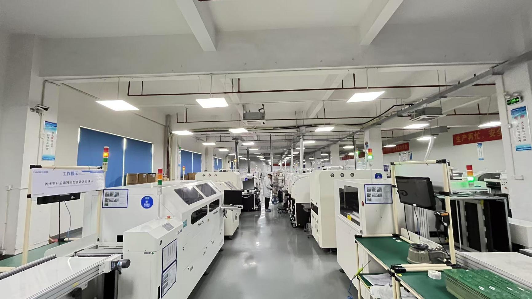
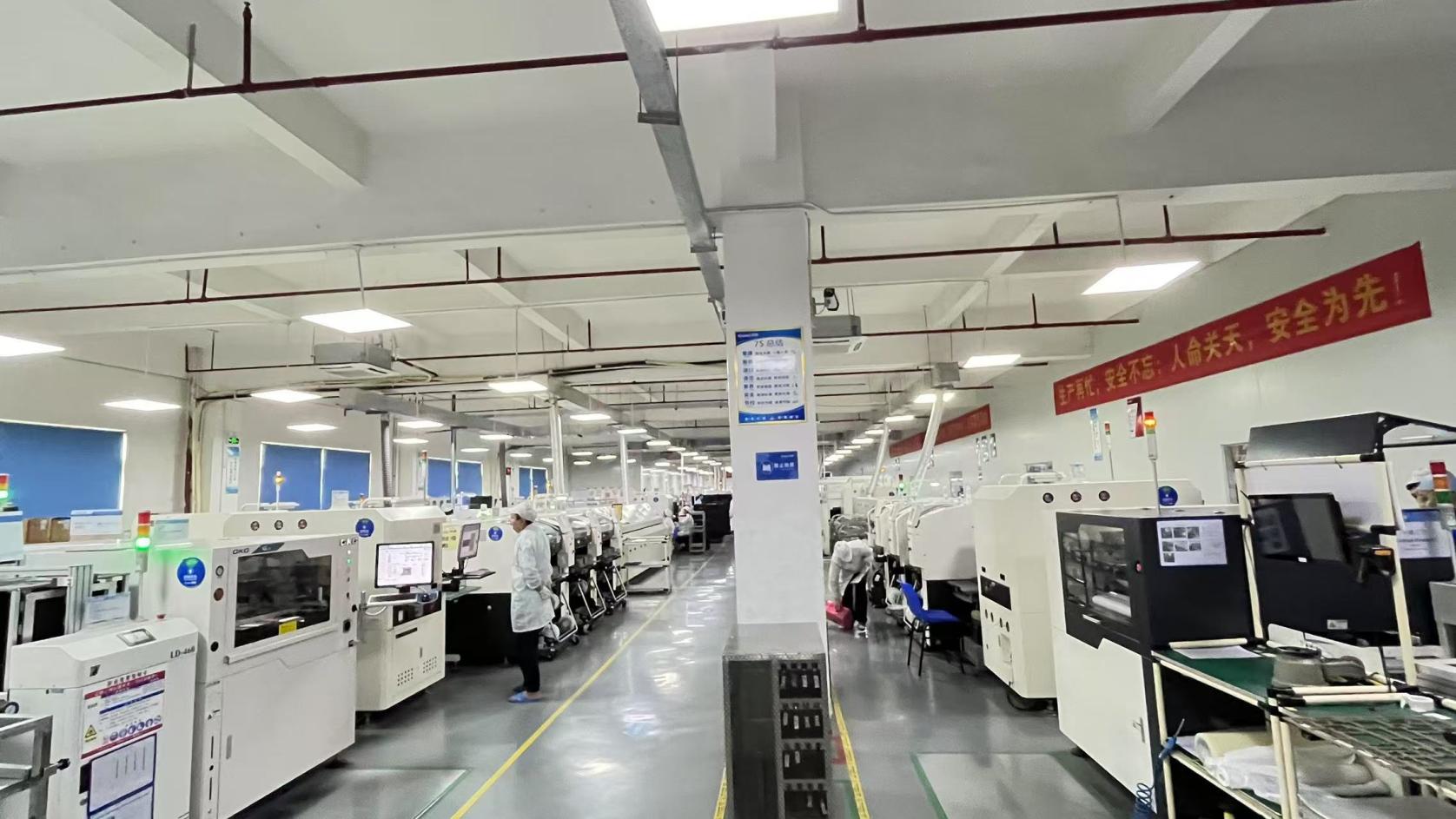
Vorynex ensures that every PCB exported to Japan undergoes multi-stage inspections, guaranteeing performance in long-lifecycle industrial controllers.
Utilizes multi-angle camera arrays to compare component placement and solder joints against CAD netlists, eliminating manual inspection fatigue and solder bridge defects.
Every memory module and critical control PCBA is subjected to thermal cycling chambers (-40°C to +85°C) to accelerate latent chip faults before dispatch to Japan.
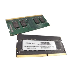
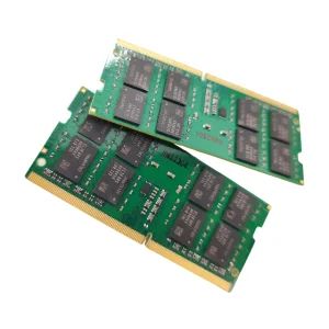
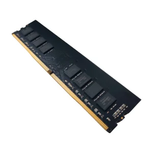
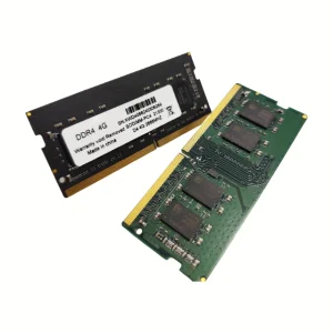
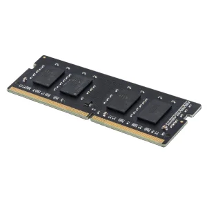
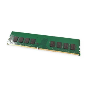
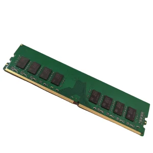
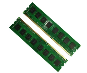
Memory modules (DDR3, DDR4, DDR5) undergo rigorous compatibility matching across multiple Japanese industrial motherboard chipsets (including Intel, AMD, and ARM architectures).
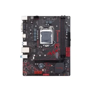
We optimize our product configurations to seamlessly drop into Nagoya’s local manufacturing lines. For example, our Inverter welding machine IGBT driver boards are customized for heavy metal stamping and robotic welding systems used in automotive frame lines. Similarly, our high-density ECC DDR4 RAM modules serve as the processing backbone for local automated guided vehicles (AGVs) operating in warehouse hubs, ensuring zero memory-fault crashes.

Compare our standard parameters engineered for demanding industrial, aerospace, and robotics networks.
| Parameter Category | Technical Specification Details | Nagoya Industrial Compliance Standard |
|---|---|---|
| Base Laminate Material | FR-4 High-Tg (KB6160, S1000-2M), Aluminum Clad, High-Frequency Rogers | JIS C 6484 Compliant for high-stress automation |
| PCB Surface Finishes | Lead-Free HASL, ENIG, Immersion Silver, OSP (Organic Solderability Preservatives) | RoHS 3.0 & WEEE Directive Compliant (Lead-Free Leadout) |
| Component Placement Precision | SMT capability down to 01005 components, BGA pitch down to 0.35mm with micro-via design | Zero-defect placement on multi-axis controller boards |
| Memory Form Factors | DDR3, DDR4, DDR5 (UDIMM, SODIMM, ECC-Unbuffered, ECC-Registered) | IPC-A-610 Class 3 for Medical & High-Availability Computing |
| Thermal Cycles Test Protocol | 100 cycles thermal shock chamber (-50°C to 125°C) | JASO D001 Automotive electronics testing reference |
| Maximum Layer Count | Up to 32 layers for high-speed multi-bus processing platforms | Ultra-dense packaging for modern CNC & robotic controllers |
High-speed server RAM modules, specialized industrial drivers, and universal desktop memory optimized for Nagoya's smart production systems.
Addressing technical and logistics questions from Japanese procurement managers and system engineering departments.
For urgent prototypes, air cargo shipments via Shenzhen/Guangzhou to Chubu Centrair International Airport (NGO) take 2-3 business days. Bulk ocean shipments destined for the Port of Nagoya typically require 7-10 days transit time. We manage all export clearance and supply all necessary certificate documentation, including COO (Certificate of Origin), to ensure seamless Japanese customs import processing.
Our specialized lab uses advanced chipset emulation software to test PCBA and DRAM modules on target boards. In addition to IPC Class 3 quality inspection standards, we support firmware customization, JEDEC compliance configuration, and custom heat sink designs to match structural envelopes of major Japanese manufacturers.
Absolutely. Our R&D team of 180+ engineers focuses specifically on mechanical layout adaptations, impedance analysis, and structural reinforcement. We offer polyimide substrates, flex-rigid circuit geometries, and epoxy-filled vias to ensure that boards installed in heavy industrial multi-axis robotic arms withstand high gravitational and torsional forces over long operational lifetimes.
Every memory stick undergoes 100% full functional test runs under stressful software loads. We utilize advanced system-level testing along with automated optical inspection (AOI) to trace and prevent solder micro-voids, and apply specialized high-temperature aging chambers to screen out memory ICs that fail under extreme thermal stress.
Get in touch with our design engineers. We provide free engineering checks (DFM reviews) for new PCB layouts and can offer competitive quotes tailored for Nagoya's demanding technological ecosystem.
Send Inquiry Now