Explore our leading high-performance motherboard units and advanced memory modules engineered for industry-level PCBA and SMT precision operations.
In the highly precise ecosystem of Surface Mount Technology (SMT) and Printed Circuit Board Assembly (PCBA), Laser Cutting Stencils serve as the foundational blueprint. A micro-step variation in the aperture opening of a stencil can trigger major defects down the assembly line—leading to solder bridging, insufficient wet paste transfer, or micro-voids. As global technology transitions toward micro-miniaturized architectures like 01005 passives, ultra-fine pitch Ball Grid Arrays (BGAs), and high-density connectors (such as the LGA1700 CPU Socket framework), the demand for ultra-precise laser cutting stencil suppliers has skyrocketed.
Historically, chemical etching was the dominant fabrication method. However, modern high-density interconnect (HDI) designs require tolerances that only advanced fiber laser systems can execute. Top-tier stencil manufacturers now leverage specialized laser machines operating with positioning accuracies within ±2 microns. By applying advanced optical beam shaping, these factories produce stencil aperture walls with exceptionally low roughness, facilitating smooth paste release.
High-yield SMT printing relies on mechanical accuracy, material science, and design engineering:
Procuring high-quality SMT tooling and related semiconductor products is a critical challenge for global purchasing managers. High-density designs demand reliable, high-yield manufacturing. To help procurement teams navigate these standards, here is a detailed breakdown of different stencil technologies, materials, and application guidelines:
| Stencil Type | Base Material | Ideal Application / Pitch | Aperture Wall Quality | Cost Factor |
|---|---|---|---|---|
| Standard Laser-Cut | Stainless Steel (SUS304) | ≥ 0.5 mm pitch QFP, SOIC, Passives | Good (Standard deburred) | Baseline Economy |
| Fine Grain (FG) Laser-Cut | Fine-Grain Steel (e.g., Datum) | 0.4 mm pitch, fine CSPs & BGAs | Excellent (Enhanced release) | Moderate Premium |
| Step-Up / Step-Down | FG or Hybrid SUS | Mixed boards (Micro-BGAs + RF Shields) | High precision depth profiles | High Premium |
| Electroformed Nickel | Pure Electrodeposited Nickel | < 0.3 mm pitch, ultra-dense HDI | Mirror finish (Atomic smoothness) | Maximum Cost |
When validating a new laser-cut stencil factory or partner supplier, procurement teams must look beyond unit price. Long-term reliability is shaped by three main parameters:
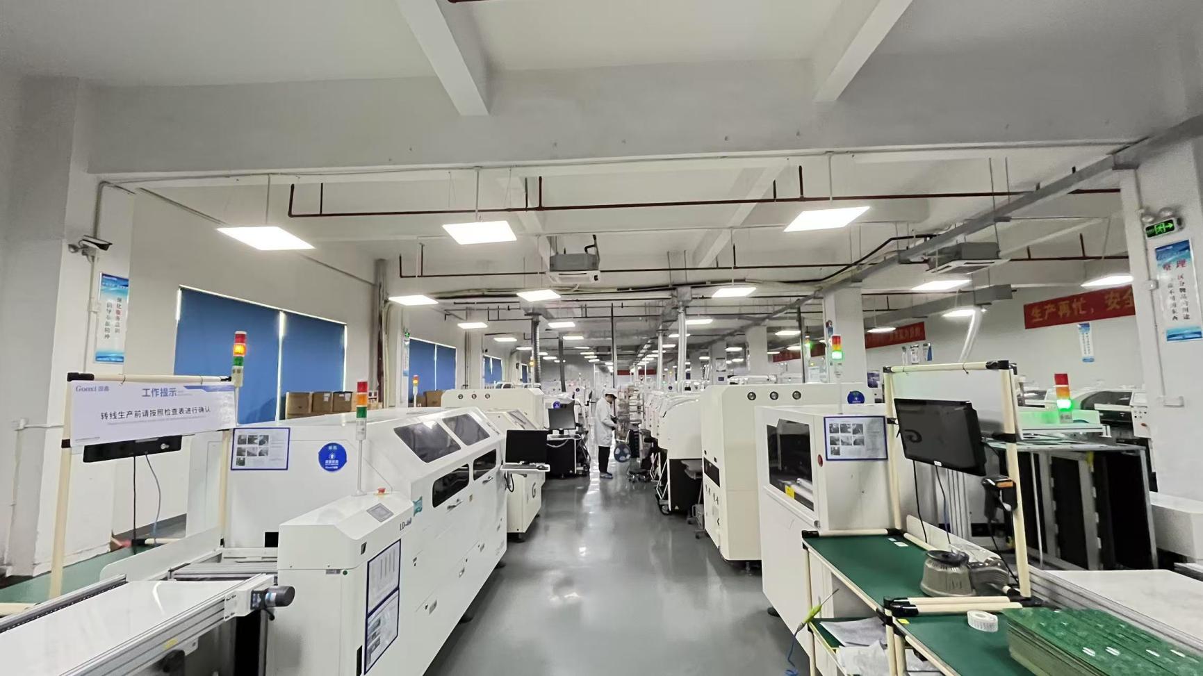
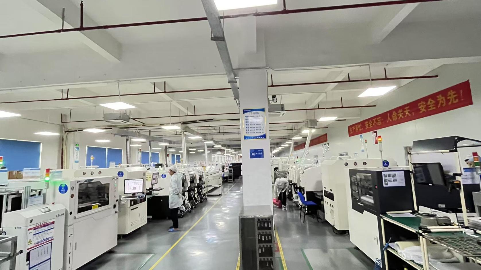
As a prominent OEM/ODM solution provider, Vorynex Memory Technology (China) Co., Ltd. represents the technological edge of China's automated manufacturing sector. Established in 2016 and backed by over 12 years of industry experience in semiconductor and memory module design, Vorynex has optimized its production lines to meet strict international demand. The factory operates a high-efficiency facility specializing in high-speed, energy-efficient memory solutions for gaming, industrial, and enterprise applications.
Backed by 180 R&D engineers, Vorynex continuously refines PCB design, frequency tuning, thermal performance, and firmware optimization, introducing roughly 240 new product models annually.
A specialized team of 45 QC staff runs 100% functional, aging, compatibility, and high-temperature stress tests using Automated Optical Inspection (AOI) and In-Circuit Testing (ICT).
With 6 years of export experience and a network of 1,200+ supply chain partners, Vorynex delivers reliable logistics and component sourcing to major global markets.
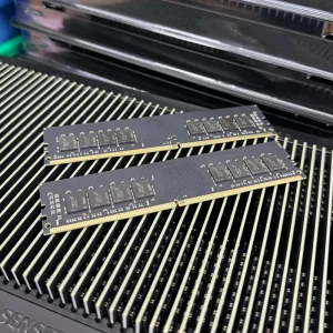
To maintain stable production yields for high-speed DDR5 modules and multi-layer PCBA units, Vorynex relies on top-tier laser-cut stencils. The transition from legacy SMT stencil designs to nano-coated step stencils has played a major role in achieving low assembly defect rates (measured in DPMO).

Different assembly projects require distinct stencil parameters. Below are common configurations based on localized SMT applications:
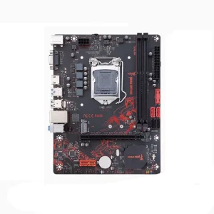
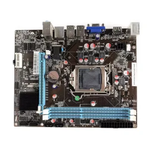
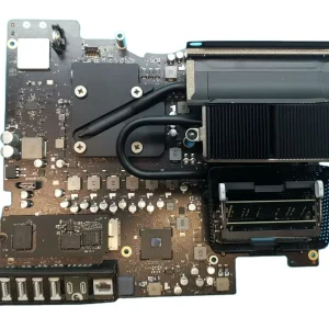
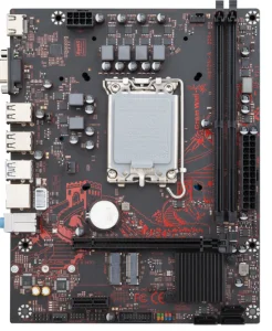
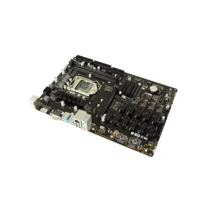
Motherboards feature a mix of large thermal ground pads, standard pitch ICs, and fine-pitch processor sockets (like the LGA1700). Applying the same solder volume across all these components is a common assembly challenge.
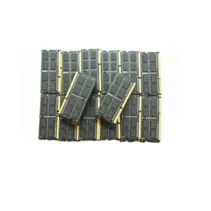
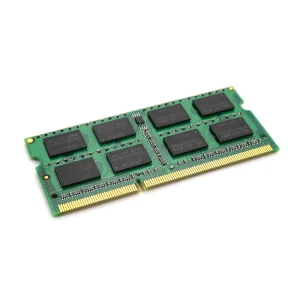
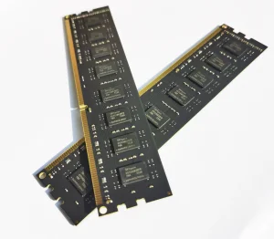
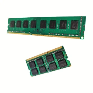
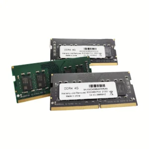
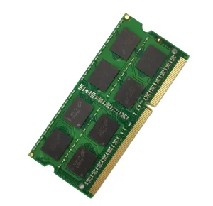
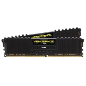
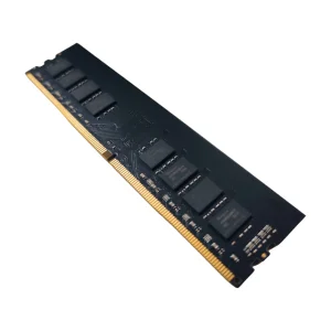
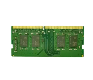
Memory stick assemblies require precise, repeatable solder paste deposition. Because the solder pads are small and closely spaced, standard stencils are prone to paste bridging.
SMT laser-cut stencils typically range in thickness from 0.08 mm to 0.25 mm (3 mil to 10 mil). The ideal thickness is determined by the pitch of the finest components on the PCB assembly. For example, boards containing fine-pitch BGAs (such as high-speed DDR4 or DDR5 RAM modules) generally require thinner stencils (0.10 mm to 0.12 mm) to prevent bridging and ensure optimal paste transfer efficiency.
The Area Ratio is the area of the aperture opening divided by the surface area of the aperture walls. Under the IPC-7525B standard, this ratio must be greater than 0.66 to ensure reliable paste release. If the ratio falls below 0.66, surface tension causes the solder paste to stick to the aperture walls, resulting in incomplete deposition and potential solder-joint defects.
Hydrophobic and oleophobic nano-coatings repel solder flux, preventing wet paste from adhering to the bottom of the stencil. This reduces cleaning frequency (from every 3-5 prints to every 30-50 prints), minimizes paste smearing, and improves printing consistency on micro-BGAs and fine-pitch passive components.
Fine-grain (FG) steel is recommended for high-density boards containing components with pitches smaller than 0.5 mm. FG steel has a uniform micro-structure that produces cleaner cuts, sharper aperture edges, and smoother walls during laser processing. Standard SUS304 remains a cost-effective choice for general-purpose electronic assemblies.
Framed stencils feature a permanently mounted mesh frame, providing excellent stability and tension for high-volume production runs. Frameless stencils consist of a loose foil designed for reusable pneumatic clamping systems (like the VectorGuard system). Frameless options reduce storage requirements and shipping costs, making them popular for prototype batches and medium-sized production runs.
Step stencils feature varying thicknesses across the same metal foil, created through chemical etching or micro-milling. Step-down areas reduce solder paste volume for fine-pitch components (like micro-controllers), while step-up areas deposit extra solder paste for larger power connectors and RF shielding. This enables custom solder volume delivery across diverse component layouts.
Stencil manufacturers require PCB design files in standard Gerber (RS-274X or Gerber X2) or ODB++ formats. Typically, designers supply the solder paste layers (usually named top paste/cream or bottom paste/cream), along with copper and silk-screen layers for component reference and fiducial matching.
Laser cutting creates microscopic burrs and slag on the stencil's underside and aperture walls. Electropolishing chemically removes these imperfections, smoothing the steel surface. This process reduces frictional resistance, helping the solder paste release cleanly onto the circuit board.
Under normal operating conditions and regular cleaning, a standard framed laser-cut stencil can reliably support 50,000 to 100,000 printing cycles. Lifespan depends on cleaning solutions, squeegee pressure, and board design (e.g., sharp component edges can accelerate stencil wear).
Chinese laser-cut stencil factories typically process files and fabricate stencils within 24 to 48 hours. By utilizing express air shipping (such as DHL, FedEx, or UPS), global delivery to Europe, North America, or Southeast Asia can be completed in 3 to 5 business days, ensuring minimal production delays.
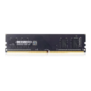
View our complete range of DDR4, DDR5, and specialized industrial memory solutions designed to optimize high-density electronic assemblies.