Explore our state-of-the-art printed circuit boards and integrated processing modules engineered for high durability and performance.

How Vorynex Memory Technology pioneers high-density multilayer integration.
As the global demand for electronics pivots toward higher computational bandwidth, smaller form factors, and stricter signal integrity, selecting an integrated manufacturing partner is paramount. Vorynex Memory Technology (China) Co., Ltd. stands at this critical nexus, offering seasoned expertise not just in high-speed DRAM modules, but in complex multilayer PCB engineering and OEM/ODM system design. Founded in 2016, Vorynex has synthesized 12 years of industry experience in semiconductors with 6 years of robust international trade experience to build a modern, high-precision electronic manufacturing infrastructure.
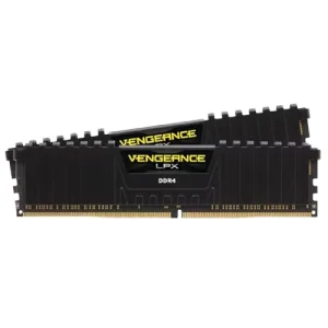
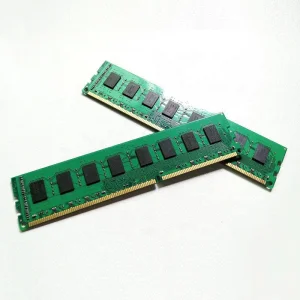
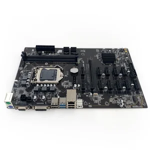
Operating a modernized smart production facility, we cater specifically to global enterprises demanding Tier-1 reliability. We combine advanced substrate processing, high-density interconnect (HDI) PCB manufacturing, SMT assembly, and semiconductor packaging optimization. By operating at the intersection of PCB fabrication and component-level system design (including DDR4, DDR5, and custom motherboards), we eliminate the common supply chain disconnect between board layout designers and semiconductor assemblers.
Harnessing automated manufacturing to deliver cost parity without compromising on quality.
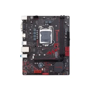
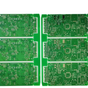
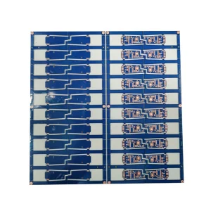
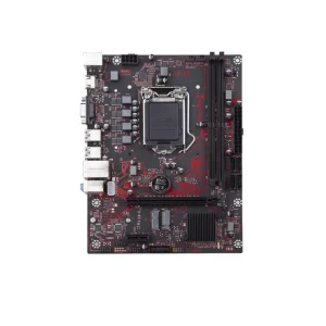
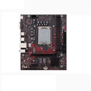
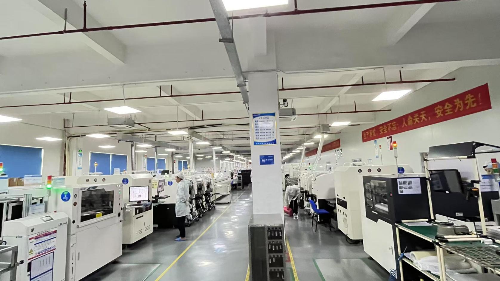
The core capability of our China facility lies in our high-density production environment. Spanning custom SMT lines, automated optical inspection (AOI) rooms, and in-circuit testing (ICT) chambers, our facility acts as a model of contemporary factory automation. By utilizing high-speed Yamaha and Panasonic SMT pick-and-place equipment, we achieve sub-millimeter component placement accuracy, crucial for tight pitches found on modern DDR5 modules and B250/H510 motherboards.
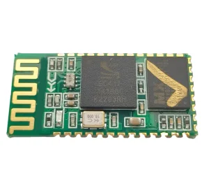
Our surface-mount lines are optimized for high-mix, high-volume production runs. We handle everything from passive 0201 packages up to ultra-fine-pitch Ball Grid Arrays (BGAs) with spacing down to 0.35mm. Our reflow ovens utilize nitrogen (N2) environments to prevent oxidation, ensuring pristine solder joints and strong mechanical connections for high-reliability components, such as those found in industrial-grade gold metal detectors and server motherboards.
Under the watch of our 45-person Quality Control team, we utilize a multi-stage validation framework:
Every single unit undergoes rigorous optical, functional, and aging validation protocols prior to export.
Direct partnerships with major semiconductor and laminate suppliers prevent supply chain bottlenecks.
Aggressive R&D cycle output keeps your hardware relevant with modern DDR5 and motherboard specifications.
Pushing the limits of high-frequency materials, HDI microvias, and low insertion-loss substrates.
The electronics industry is transitioning toward PCIe Gen 5/6, DDR5 high-speed memory architectures, and complex IoT sensor arrays. This requires significant innovation in substrate technology. Raw FR-4 is no longer sufficient for high-speed multi-gigabit routing. Vorynex’s engineering team actively designs next-generation PCBs to combat signal degradation, thermal buildup, and structural stress.
To scale down the footprint of high-performance gaming boards and complex IoT circuit assemblies, we utilize HDI technology featuring blind, buried, and stacked microvias (laser-drilled down to 0.1mm). This allows for higher routing density per square millimeter, reducing layer counts while maintaining superior signal performance. This design is crucial for our double-layer and multilayer boards built for projectors, mobile hardware, and industrial computing systems.
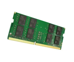
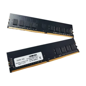
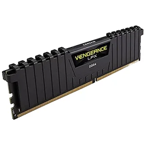
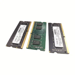
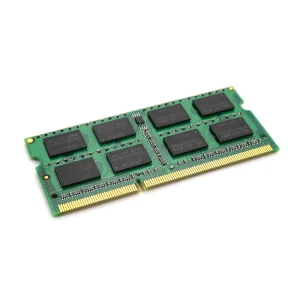
For high-frequency memory modules running at 4800MT/s to 6400MT/s and beyond, trace geometry must be strictly controlled. We maintain impedance tolerances within +/-5% (and up to +/-3% upon request) through precise track routing and high-grade low-loss laminate substrates (such as Shengyi or Rogers). High Glass Transition Temperature (High Tg 170+) laminates ensure that our PCBs maintain structural integrity during lead-free HASL or ENIG assembly steps and subsequent operational thermal cycles.
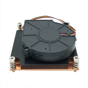
As server motherboard designs shrink and processors dissipate more power, thermal vias, heavy copper tracking, and integrated copper coins are embedded directly within our multilayer substrates. This configuration permits fast thermal dissipation from high-heat components (such as CPU voltage regulator modules or high-power server chips) directly into integrated chassis heat sinks, prolonging device life spans.
Tailored engineering designs addressing the complex demands of distinct high-reliability sectors.
Each industry segment imposes unique electrical and physical constraints on its hardware. Our multidisciplinary engineering and QC teams possess deep vertical knowledge, allowing us to align production techniques with target certifications.
We supply server-grade motherboards, memory modules, and expansion cards engineered for high-availability datacenters. Our products feature low-latency trace routes, high reliability under continuous operation, and robust error-correcting code (ECC) capabilities. These qualities ensure minimal server downtime and prevent data corruption during enterprise read/write cycles.
Industrial environments present vibration, dust, and electrical noise. We manufacture high-sensitivity PCBs for industrial detectors (e.g., gold metal detectors, sensor arrays) using custom shielding and conformal coatings. This shields the circuit from electromagnetic interference (EMI) and harsh operational environments, maintaining reading accuracy and longevity.
With smart vehicles driving the modern automotive sector, PCBs must meet the stringent IATF 16949 quality system. From ADAS sensors to infotainment mainboards, Vorynex implements selective thermal dissipation, thick copper layers for high power demands, and robust thermal cycling tests to ensure components withstand the temperature swings of vehicle environments.
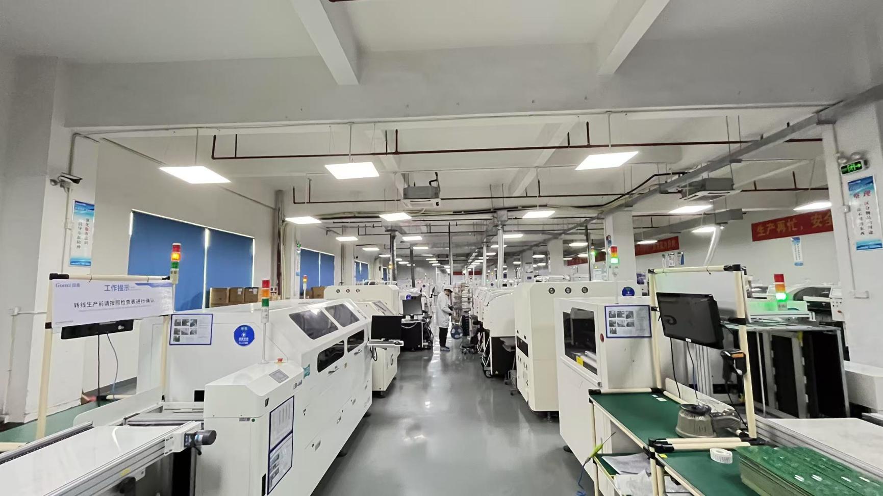
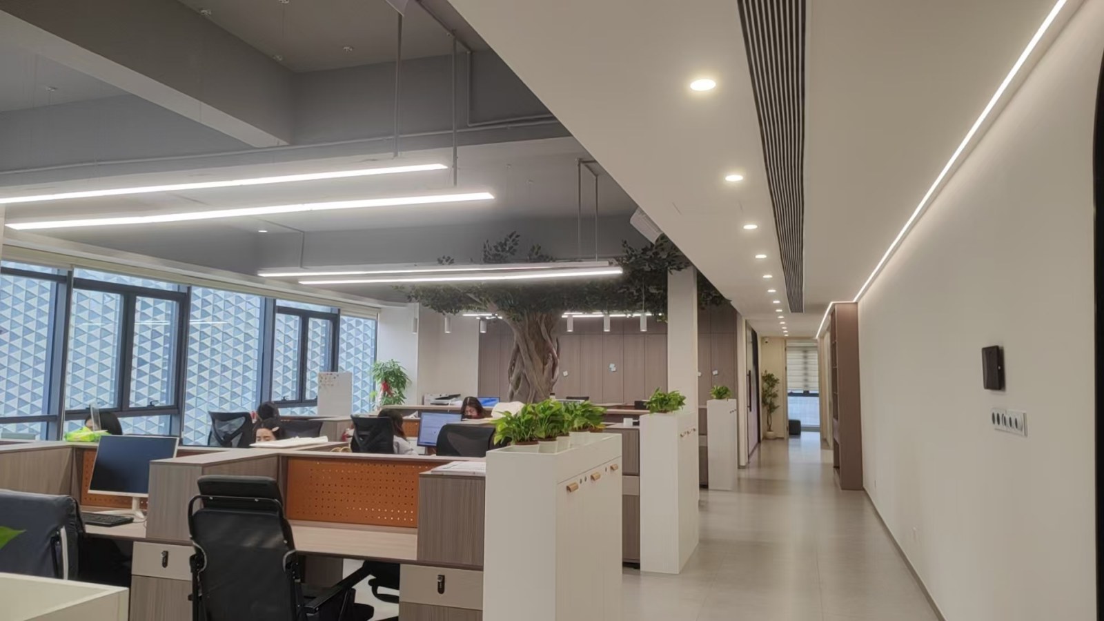
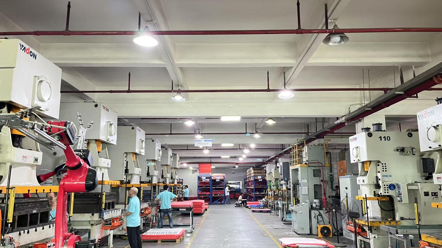
A glimpse into our high-speed SMT assembly, testing, and component storage facilities.

Navigating regulatory landscapes, quality standards, and logistics to ensure seamless delivery.
For international buyers, the challenge of sourcing from China isn't merely the quality of manufacturing; it's the complex web of cross-border compliance. Vorynex actively solves these points by maintaining certifications such as RoHS, CE, FCC, and REACH. This ensures that all components, solder alloys, and substrates used in our factory are lead-free, non-toxic, and fully cleared for distribution within North America, Europe, South America, and the Asia-Pacific region.
With an annual export volume reaching millions, we maintain close partnerships with major global forwarding networks. We offer comprehensive support for custom duties, tariff code classifications (HS Codes), and secure packaging formats. Our components are sealed in vacuum-packed anti-static ESD bags with moisture indicator cards, preventing damage from humidity during long sea or air transits.
To eliminate time-zone communication barriers, our account managers are grouped into specialized regional divisions. We offer transparent DFM (Design for Manufacturability) analysis during the quotation phase, identifying layout flaws or component availability risks before production begins. This shortens prototype approval cycles and speeds up time-to-market.
Answers to critical questions regarding PCB fabrication, testing, and component logistics.
Discover our selection of industrial PCBA layouts, high-performance DRAM memory, and thermal dissipation systems.